Some people seem to think being in the industry makes you infallible. Plenty of people get their own industries wrong. That’s why companies make bad bets and lose competitions. Industry insight is extremely valuable and insiders should obviously know more than the average bystander but that does not make them prophets. This is why discussion and the thinking and reasoning behind it is still indispensable.is he the only person in the industry here or something?
You are using an out of date browser. It may not display this or other websites correctly.
You should upgrade or use an alternative browser.
You should upgrade or use an alternative browser.
Chinese semiconductor thread II
- Thread starter vincent
- Start date
It is a pattern I've noticed for foreign professionals in semi. It certainly does seem that Chinese secrecy on its semi industry is paying dividends.I think he is mostly memeing because hvpc is one of the more week known individuals here with similar skeptical sentiments, but I think what is a legitimate common trait being implied, is the inability to recognise and track Chinese side semiconductor rumours in a competent manner, and reliance on "official" releases of information as a gauge of actual progress or state.
In that sense, it is less so much that hvpc and this person are similar and more that that type of thinking is the usual way of tracking Chinese semi development by the majority of foreign observers, professional or not.
Do you think I know everything that is ongoing in [REDACTED SEMICONDUCTOR COMPANY] ? Let alone the entire European scene?It is a pattern I've noticed for foreign professionals in semi. It certainly does seem that Chinese secrecy on its semi industry is paying dividends.
Not everyone who works for think tanks says bullshit due to their lack of knowledge. Some of them simply do it for money because they are paid to create a certain narrative and opinion among the public. The way he post things, very much sound like someone who would work for such a think tank.I don't know man, as much I disagree with hvpc in A LOT of things he seems to be a bit more knowledgeable than this, this is think tanker level of thinking man.
He had an account here for several years but didn't post anything. Then first time he posted he started asking questions like How many 28nm machines have SMEE shipped? Are they being used in SMIC/YMTC? Which cities Huawei constructing their fabs? He said he was doing research for investing in semi companies. Then few days later he claimed to have insider knowledge more than anyone else, which would make those questions pointless. If someone posts expert information here and the others are convinced that he is an insider, the other insiders are more likely to share information with them that they would not share in the public.
Last edited:
SMSC finished construction of the building for their fab expansion late last year. Would they have continued the construction of the building if they didn't have a way to get tools for the fab? They had already been sanctioned for a long time already. Before they even started erecting the building. I think they basically cannot get any technical support or machine tools from Western tool makers at this point for that fab. Because of US sanctions. Yet they still built it. They must know something we don't.
Sales of devices with the HiSilicon Kirin 9000S keep increasing and it seems like they are even making huge AI chips in SMIC's N+2 process at SMSC.
YMTC and CXMT also built their fab expansions but seem to have developed types of memory which are just below the sanctioned limit so they can still use imported tools. But this wouldn't apply to SMSC.
Earlier this month YMTC got listed as a Chinese Military Company by the US DoD. What are the differences of being listed as a military company vs being listed in the entity list like SMIC? Would YMTC still be able to purchase tools if they keep the node below US limits?YMTC and CXMT also built their fab expansions but seem to have developed types of memory which are just below the sanctioned limit so they can still use imported tools. But this wouldn't apply to SMSC.
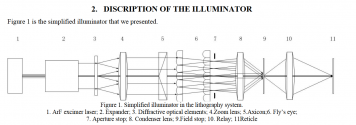
The guy in the post talk about the micromirror array illuminator of the lithography that due patterning and overlay reasons has to send the light to the wafer in different shapes for efficiency because sadly for us nature decided to slap fab workers in the face and be a wave and particle at the same time, so you have to find workarounds to increase the resolution of your optical fabrication tools.
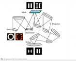
The I saw this guy tweet bragging about the FlexRay MEMS <lets keep in mind that> micromirror array. Pretty neat technology to be honest the closest thing to maskless DUV lithography and also one the early use of advance packaging.
"FlexRay and Tachyon SMO are two key, complementary ingredients in ASML’s holistic lithography portfolio."
Back in the day when the first SMEE ArF scanner was out they where using microlenses.
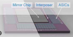
I thought to myself wow, they got me there, who is supplying this in China? Well China has two big MEMS manufacturers SAI micro and SMEC, they have advance packaging companies and they have fabs that can make ASIC chips 28nm down to 7nm. All boil downs to logic.
So yes looks like that China has narrow down on this technology and they recently published a paper discussing this tech.
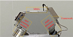
Statement of one the micro-mirror mems manufacturers in China:
"international operation of high-end integrated circuit wafer foundry manufacturers, but also domestic with independent intellectual property rights and master the core semiconductor manufacturing technology of the characteristics of the process of professional wafer manufacturers. The company has many pilot platforms and mass production factories at home and abroad, and its business covers the world. Its service customers include internationally renowned DNA/RNA sequencer, lithography machine, computer network and system, silicon photon, infrared, wearable equipment, new medical equipment, automotive electronics and other giant manufacturers, as well as leading enterprises in the sub industry, The product range covers many fields such as communication, biomedical, industrial automobile, consumer electronics, etc. At the same time, the company is building advanced wafer-level packaging and testing capabilities, is committed to providing customers with systematic high-end manufacturing services from process development, wafer manufacturing to packaging and testing, and strives to develop into a well-known semiconductor manufacturing leader with international operations. "
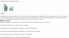
holistic lithography:
based on the bid filings for SN2 building, it won't only until Q3 at the earliest. So production probably starts Q4 at the earliest. If they can fully utilize SN1's 35k wpm, by end of this year, it will be pretty good progressSMSC finished construction of the building for their fab expansion late last year. Would they have continued the construction of the building if they didn't have a way to get tools for the fab? They had already been sanctioned for a long time already. Before they even started erecting the building. I think they basically cannot get any technical support or machine tools from Western tool makers at this point for that fab. Because of US sanctions. Yet they still built it. They must know something we don't.
Sales of devices with the HiSilicon Kirin 9000S keep increasing and it seems like they are even making huge AI chips in SMIC's N+2 process at SMSC.
YMTC and CXMT also built their fab expansions but seem to have developed types of memory which are just below the sanctioned limit so they can still use imported tools. But this wouldn't apply to SMSC.
auto chip module installation changes in China market from 2022 to 2023
Keep in mind many of the purchases from foreign chipmakers are by Tesla & legacy JVs. Among Chinese standalone brands, the Chinese chipmaking market share is even higher than this
Keep in mind many of the purchases from foreign chipmakers are by Tesla & legacy JVs. Among Chinese standalone brands, the Chinese chipmaking market share is even higher than this
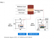
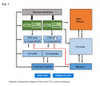
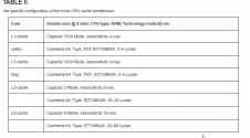
Novel CPU cache architecture based on two-dimensional MTJ device with ferromagnetic Fe3GeTe2
With the development of Artificial Intelligence (AI) in recent years, the fields of computer, biology, medicine, and aerospace have demanded higher requirements for the processing and storage of information. In this paper, a novel Magnetic Tunnel Junction (MTJ) based Spin-Orbital Torque Magnetic Random Access Memory (SOT-MRAM) composed of Fe3GeTe2 (FGT) is employed as a storage medium in the computer architecture. On the basis of the analysis of the fundamentals, model configuration, characteristics and performance advantages of the FGT based SOT device, a hybrid storage (L1, L2, Last Level Cache) is constructed, with FGT-SOT-MRAM, conventional SOT-MRAM and STT-MRAM replacing the original static random access memory (SRAM) in the novel triple-level CPU cache architecture. This can override the increasing leakage problem of SRAM, while opening up the application of two-dimensional van der Waals ferromagnets in computer systems at the L1 cache level. Meanwhile, an innovative cache optimization scheme is put forward for magnetic memory to better match the performance of FGT-SOT-MRAM to CPU. The simulation results demonstrate that the FGT-based MRAM can achieve up to 38.03% IPC optimization and 53.41% power optimization in the CPU cache system in contrast to the conventional ones.
