Chinese semiconductor thread II

gelgoog

Lieutenant General
Registered Member
They are probably overestimating the increase in capacity by CXMT. Ever since they changed their fab design from the original plan it makes it harder to estimate the increase in production capacity. I doubt it will go all the way to 300k wpm without building more fab space.

A bigger question, at least to me, is what about Fujian Jinhua (JHICC) or the DRAM fabs which were supposed to be built by Unigroup. JHICC won its lawsuits against the US government and settled with Micron.
Please, Log in or Register to view URLs content!

The US government no longer has an excuse to ban sales of semi tools to JHICC.
 
Last edited:

tokenanalyst

Brigadier
Registered Member

Jingsheng Electromechanical: Achieved a breakthrough in the localization of 8-12 inch semiconductor large silicon wafer equipment​


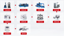
According to the investor relations activity record sheet disclosed by Jingsheng Electromechanical, the company has actively deployed the research and development of large silicon wafer manufacturing, chip manufacturing, packaging and other equipment in the field of semiconductor equipment, and has gradually achieved a breakthrough in the localization of 8-12 inch semiconductor large silicon wafer equipment. The relevant products have been sold in batches and widely recognized by downstream customers. At the same time, based on the extension of the industrial chain, the company has developed 6-8 inch silicon carbide crystal growth equipment, slicing equipment, thinning equipment, polishing equipment and epitaxial equipment in the field of power semiconductors to achieve domestic substitution of silicon carbide epitaxial equipment. In the field of photovoltaic equipment, the company's products cover silicon wafers, batteries and components, providing customers with photovoltaic full-line solutions. During the reporting period, the battery cell equipment independently developed by the subsidiary Zhejiang Jingsheng Photonics Technology Co., Ltd. was successfully exported to overseas customers. In addition, the company actively deployed new material businesses in the pan-semiconductor field, and gradually developed high-purity quartz crucibles, sapphire materials, silicon carbide materials and other material businesses with broad application scenarios.

1730816127246.png

Please, Log in or Register to view URLs content!
 

tokenanalyst

Brigadier
Registered Member

AMEC applies for patent for dual-chamber processing system and gas supply method​


The patent abstract shows that the present invention discloses a dual-chamber processing system and a gas supply method, including: two processing chambers, respectively used to perform process treatment on the substrates placed therein. A main air inlet channel is connected to a process gas source, and is used to transport the process gas in the process gas source to the two processing chambers. A gas flow regulating component is arranged on the main air inlet channel, and includes at least one gas diverter. A flow adjustment control unit is used to control the gas flow regulating component according to the substrate processing results of the two processing chambers to adjust the process gas flow entering the two processing chambers. The present invention can solve the problem that the gas pressures of the two processing chambers are different due to the inherent problems of the gas outlet of the dual-chamber processing system, which in turn leads to inconsistent etching rates in the two processing chambers.

Please, Log in or Register to view URLs content!
 

tokenanalyst

Brigadier
Registered Member

Diamond laser technology has achieved a major breakthrough​


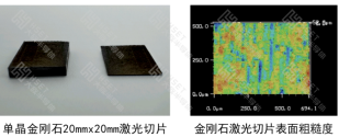
Han's Semiconductor has made an important technological breakthrough in the field of diamond slicing, launching the QCBD laser slicing technology and related equipment, which has achieved high-quality, low-damage and high-efficiency laser slicing of diamonds. This achievement marks an important progress in laser slicing technology in diamond material processing, filling the domestic technological gap in this field.

Through precise control of laser energy and modulation of beam shape, Han's Semiconductor has overcome the processing difficulties caused by the large angle between the diamond cleavage plane {111} and the slicing direction {100}, and achieved high-precision, low-damage peeling of the ingot. According to research data from Han's Semiconductor's QCB research laboratory, using this technology, the roughness Ra after peeling is as low as 3μm, and the laser damage layer can be greatly reduced to 20μm. This technological breakthrough will significantly reduce the processing cost of diamond and promote its widespread application in high-end fields such as electronics and optics.

1730816606193.png

Please, Log in or Register to view URLs content!
 

tokenanalyst

Brigadier
Registered Member

Wuxi Semiconductor Equipment Company Completes Series B Financing​


Wuxi Xingwei Technology Co., Ltd. completed a B round of financing of tens of millions of yuan, with investors including Shangqi Capital and old shareholder Yida Capital. This round of funds will be mainly used for R&D iteration, team improvement and market expansion, and promote technological innovation of key components of domestic semiconductor equipment.

tar Micro Technology was founded in 2015 and is headquartered in Wuxi. It has a research and development center in Shanghai, a South China service center in Shenzhen, and an overseas business department in Tokyo. The company focuses on the research and development of leading precision motion control solutions in the semiconductor industry.

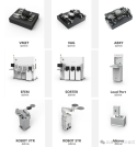
The company's R&D team has more than 100 members, over 100 related patents, and has shipped more than 1,500 self-developed motion platforms and more than 200 self-developed wafer transfer systems.High-precision motion platforms and wafer transfer equipment are two key components of semiconductor equipment and are also XIVI's two main products. XIVI can provide modular and customized products and services, flexibly adapting to the personalized needs of different customer scenarios while ensuring efficient and stable system performance.

Recently, the company released its latest product, the vacuum manipulator. As a substrate handling robot in the wafer vacuum transfer system, the XIVI vacuum manipulator's full-link arm mechanism adopts a fully closed-loop control method, which can achieve higher positioning accuracy, faster response time, and higher work efficiency.

1730817521925.png

Please, Log in or Register to view URLs content!
 

AndrewS

Brigadier
Registered Member
Did anyone forsee Korean semiconductors getting slaughtered so early? I expected it to take years yet it's happening right now.

Must be painful for Koreans. They talked about fighting China but they can't even handle their Fujian subsidiary.

Semiconductor fabs are a boom and bust industry.

So as soon as the downturn hit, we all knew it was non-Chinese fabs that would see orders dry up first, as Chinese companies can't rely on semiconductor imports which are at risk of sanctions.
 

tokenanalyst

Brigadier
Registered Member
Semiconductor fabs are a boom and bust industry.

So as soon as the downturn hit, we all knew it was non-Chinese fabs that would see orders dry up first, as Chinese companies can't rely on semiconductor imports which are at risk of sanctions.
The Stooge sponsored semiconductor controls on China has accelerated the downturn on the semiconductor industry.
 

tokenanalyst

Brigadier
Registered Member

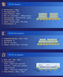
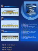
Tiancheng Advanced Technology released the "Nine-fold" advanced packaging technology platform, and the 12-inch wafer-level TSV three-dimensional integrated production line was put into operation.​

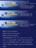
On the " Jiuzhong " advanced packaging technology platform, every tiny connection and every fine channel is a carefully crafted masterpiece, carrying a torrent of information, and interpreting Tiancheng's advanced creative ideas and struggle journey on the micro-nano scale stage.

The birth of Tiancheng Advanced's 3D TSV technology was almost synchronized with TSMC's COWOS, and the newly established Tiancheng Advanced will greatly promote domestic industrialization. Its technical route is comparable to but different from COWOS. Its ultra-high density interconnection integration solution has a line width of up to 0.4 microns, and the number of wiring layers can replace part of the PC and IC substrate wiring to a certain extent, with the number of layers reaching 6.

1730818759227.png1730818789056.png
1730818834508.png

Please, Log in or Register to view URLs content!
 

gelgoog

Lieutenant General
Registered Member
Did anyone forsee Korean semiconductors getting slaughtered so early? I expected it to take years yet it's happening right now.
Must be painful for Koreans. They talked about fighting China but they can't even handle their Fujian subsidiary.
I knew that China would start nibbling the South Koreans at the low end. What I did not expect was for Samsung to flop at the high end logic to this degree. The Taiwanese chip makers outside TSMC like UMC, Powerchip, Vanguard Semiconductor, are also likely to suffer. As the Chinese EV sector moves to self-production you will also see STMicro and Renesas drop like a stone.
 
Top