Chinese semiconductor thread II

tokenanalyst

Brigadier
Registered Member

Yaze Semiconductor Components and Quartz Materials R&D and Production Base signed a contract to settle in Wuxi​

The Yaze semiconductor components and quartz materials R&D and production base project was signed and settled in Wuxi High-tech Zone. The total planned investment of the project is 3 billion yuan .

It is reported that Beijing Yaze Quartz Materials Co., Ltd. is one of the few domestic companies that masters upstream raw material preparation technology and integrates production, R&D, and sales into a full industrial chain manufacturing enterprise. It mainly produces ultra-high purity quartz materials and products for integrated circuits, and has achieved independent control in all aspects such as raw materials, processes, and equipment.
1730907141078.png
Public information shows that Beijing Yaze Quartz Materials Co., Ltd. was established in August 2022. It adheres to the main line of electronic special materials manufacturing and has completed the A+ round in 2024. The business scope includes the manufacturing of electronic special materials, sales of non-metallic minerals and products, and the manufacturing of non-metallic mineral products. Especially in the key link of integrated circuit wafer manufacturing, Yaze has a key quartz material that can provide core technology for the 40-28 nanometer mature process and 14 nanometer advanced process of integrated circuit wafer manufacturing companies.

Please, Log in or Register to view URLs content!
 

gelgoog

Lieutenant General
Registered Member
domestic companies only occupy 15% of China market for analog chips. Majority still foreign suppliers.
annually the analog chip markets globally is over $70Billion.

This sector is mature chips and saying that China is self sufficient in mature chips is off. There's still alot of room to operate.
Did you know that Realtek typically manufactures chips at SMIC? That is one reason why you get statistics like that.
China has good software to design analog chips, and talent to design such chips exists in China already in certain niche applications like audio processing, I think if there was the demand Western analog chip imports could be replaced quickly.
 

tphuang

Lieutenant General
Staff member
Super Moderator
VIP Professional
Registered Member
Please, Log in or Register to view URLs content!

domestic companies only occupy 15% of China market for analog chips. Majority still foreign suppliers.
annually the analog chip markets globally is over $70Billion.

This sector is mature chips and saying that China is self sufficient in mature chips is off. There's still alot of room to operate.

It takes time to build up capacity and a lot of capacity is coming online in the next few years. In general, some of these articles about state of industry in China is based on dated sentiment and such.
 

tokenanalyst

Brigadier
Registered Member

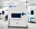
Yibai Technology delivers Micro LED wafer-level PL mass detection equipment


According to reports, the PL detection equipment for Micro LED chips shipped this time uses PL detection technology, which can achieve non-contact, non-destructive and ultra-fast luminous performance detection. The Micro PL technology mastered by Yibei can detect the brightness and spectral information of tens of millions of cores on Micro LED COW (chip on wafer) or COC (chip on carrier) wafers within minutes, and the smallest verified detectable core size is 3μm*3μm.In addition, the device also has core technologies of optical imaging, spectral acquisition and massive data analysis, which can achieve efficient and accurate abnormality judgment, and effectively solve the process control and yield monitoring problems in the production chain after Micro LED miniaturization.

1730922156811.png

Please, Log in or Register to view URLs content!
 

tokenanalyst

Brigadier
Registered Member

The Institute of Microelectronics has made important progress in advanced process simulation​


Compared with the traditional FinFET process, the gate-all-around transistor (GAAFET) introduces processes such as inner spacer and channel release, which must be achieved through precise lateral etching of the stacked structure. High-precision etching process control is one of the biggest challenges facing 3D integrated circuit manufacturing, and its process mechanism and regulation mechanism have received widespread attention in the scientific and industrial communities.

In response to the morphological defects and uniformity problems faced by the lateral selective etching process of the Si/SiGe stacked layers of the GAA inner wall structure, Chen Rui, a researcher at the EDA Center of the Institute of Microelectronics, worked with Li Junjie, a senior engineer at the Pioneer Center, Professor Wang Zhongrui of the Southern University of Science and Technology, and Professor Lado Filipovic of the Vienna University of Technology to propose a new simulation algorithm for the desorption and diffusion of Ge atoms, establish a continuous two-step dry etching process profile simulation model based on the Monte Carlo method, realize the lateral selective etching process profile simulation for the Si/SiGe six-layer stacked structure, and complete the tape-out experiment of the corresponding structure. By combining morphological simulation and transmission electron microscopy (TEM) characterization, the surface rounding phenomenon of the Ge layer etching and the influence mechanism of parameters such as cavity gas pressure on the uniformity of etching morphology were explored. This work provides theoretical and experimental references for clarifying the mechanism of the new principle etching process and optimizing process performance.

The research results were recently published in the top journal in the field of materials , Small , with the title "A Two-Step Dry Etching Model for Non-Uniform Etching Profile in Gate-All-Around Field-Effect Transistor Manufacturing". Hu Ziyi, a master's student at the Institute of Microelectronics, is the first author of the paper, and Chen Rui, a researcher at the Institute of Microelectronics, Wei Yayi, and Professor Wang Zhongrui of the Southern University of Science and Technology are co-corresponding authors. The paper was also selected for oral presentation at SISPAD 2024, the flagship conference in the field of TCAD simulation. In addition, related research results have also been published in journals such as ACS Applied Electronic Materials and Journal of Vacuum Science & Technology A , with Li Junjie, a senior engineer at the Institute of Microelectronics, as the co-corresponding author. This research was supported by the Strategic Priority Research Program of the Chinese Academy of Sciences and the National Natural Science Foundation of China.

Please, Log in or Register to view URLs content!
 

tokenanalyst

Brigadier
Registered Member

The Institute of Microelectronics' 28nm embedded RRAM IP enables advanced display chips to be mass-produced in Beijing​

Currently, Flash has encountered a bottleneck in process miniaturization, and large-scale mass production has stagnated at 40nm. The team of Academician Liu Ming from the Institute of Microelectronics has launched an innovative and groundbreaking 28nm embedded RRAM IP, which has been successfully applied to the world's first 28nm advanced display chip and achieved mass production.

Recently, Beijing Economic and Technological Development Zone (Beijing Yizhuang) Display High-tech Enterprise announced that the world's first 28nm advanced process SoC high-end display chip using 28nm RRAM IP has completed mass production in Beijing, and has been successfully applied to the Mini LED (sub-millimeter light-emitting diode) high-end TV series of domestic leading customers. This chip has a built-in RRAM (Resistive Random Access Memory) storage module. Its storage core technology and RRAM IP are developed by the Institute of Microelectronics of the Chinese Academy of Sciences, and the picture quality adjustment algorithm is developed by Yizhuang Enterprises. The mass production of this product marks the birth of the world's first advanced commercial TCON (Timing Controller) picture quality adjustment chip using 28nm embedded RRAM IP, and display chips have entered a new semiconductor process height.

Academician Liu Ming said, "The research team of the Institute of Microelectronics has conducted systematic research in the field of semiconductor storage, especially in the field of RRAM, for more than 20 years, and has created a complete independent intellectual property system from materials, processes, devices, circuits to chips and systems. This 28nm display chip was developed by the team of the Institute of Microelectronics in cooperation with Yizhuang enterprises. It has completely independent intellectual property rights and is a breakthrough in domestic display chip products. At the same time, the mass production of this chip in Beijing has created another successful example of industry-university-research cooperation, and has paved a new path for the large-scale industrial application of the 'national team' advanced integrated circuit technology."

Please, Log in or Register to view URLs content!
 
Top