Chinese semiconductor thread II

tokenanalyst

Brigadier
Registered Member

Qingting Optoelectronics' shows ultra-high precision 3D intelligent optical inspection equipment​


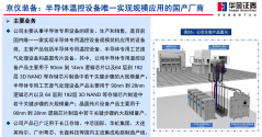
Qingting Optoelectronics exhibited the high-precision 2D+3D quantitative inspection three-light AOI equipment Weber-G3300A for semiconductor back-end packaging and testing Die Bond and post-Wire Bond Die surface defect inspection, as well as solder joint and gold wire defect inspection after gold wire bonding; Qingting Optoelectronics exhibited the wafer-level 2D+3D quantitative inspection equipment Spectra-Wafer for semiconductor advanced packaging wafer cutting before and after Die surface defects, cutting line defects and RDL defect detection, bump height and coplanarity measurement .​

1727962273427.png

Please, Log in or Register to view URLs content!
 

tokenanalyst

Brigadier
Registered Member

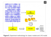
Lightweight Hotspot Detection Model Fusing SE and ECA Mechanisms​


Beijing Smartchip Microelectronics Technology Co., Ltd.,
College of Integrated Circuits, Zhejiang University

Abstract​

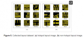
In this paper, we propose a lightweight lithography machine learning-based hotspot detection model that integrates the Squeeze-and-Excitation (SE) attention mechanism and the Efficient Channel Attention (ECA) mechanism. These mechanisms can adaptively adjust channel weights, significantly enhancing the model’s ability to extract relevant features of hotspots and non-hotspots through cross-channel interaction without dimensionality reduction. Our model extracts feature vectors through seven convolutional layers and four pooling layers, followed by three fully connected layers that map to the output, thereby simplifying the CNN network structure. Experimental results on our collected layout dataset and the ICCAD 2012 layout dataset demonstrate that our model is more lightweight. By evaluating overall accuracy, recall, and runtime, the comprehensive performance of our model is shown to exceed that of ConvNeXt, Swin transformer, and ResNet 50.​

1727964528334.png1727964545274.png

Please, Log in or Register to view URLs content!
 

huemens

Junior Member
Registered Member

China chip-packaging giant JCET takes over Shanghai plant of US flash memory maker SanDisk​

Please, Log in or Register to view URLs content!
The US$624 million deal is expected to enlarge JCET’s share in China’s data storage market
Chinese chip-packaging and testing giant Jiangsu Changjiang Electronics Tech (JCET) has completed its acquisition of an 80 per cent equity stake in the Shanghai plant of US flash memory maker SanDisk
The remaining 20 per cent equity is held by SanDisk China.
 

tokenanalyst

Brigadier
Registered Member
Naura working on High Aspect Ratio Etching using carbon mask.

High Aspect Ratio Carbon Hard Mask Etch Process for Profile and LCDU Control.​

Abstract:​

Improving the bowing profile and LCDU in HAR etching is challenging due to ion sputtering, insufficient sidewall protection, and uneven polymer deposition. To address these challenges, we investigated the gas ratio in deep hole etching of ACL, the effect of new polymer gas on sidewall protection, and the effects of different descum steps and their addition times and BRF parameters on LCDU. From the results, it can be seen that using more COS in the early stage of etching and adding polymer gas SiCl4 all have varying degrees of improvement on bowing profile. Using a descum step containing CHF3, adding it earlier and using lower BRF resulted in different levels of improvement in LCDU.​
1727967186977.png

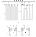
Method for manufacturing through hole in semiconductor structure and semiconductor process equipment​

CN118613056A​


Abstract

The application discloses a method for manufacturing a through hole in a semiconductor structure and semiconductor process equipment, wherein the method comprises the following steps: a carbon-containing layer, a silicon oxide layer laminated over the carbon-containing layer, and a patterned first mask layer on the silicon oxide layer, the method comprising: etching a silicon oxide layer: etching the silicon oxide layer by taking the first mask layer as a mask to form a first through hole penetrating through the silicon oxide layer in the silicon oxide layer, wherein the aperture of the first through hole gradually increases from the top of the silicon oxide layer to the bottom of the silicon oxide layer; etching a carbon-containing layer: and etching the carbon-containing layer by taking the silicon oxide layer as a mask so as to form a second through hole communicated with the first through hole in the carbon-containing layer. The application can delay the blocking time of the first through hole of the silicon oxide layer, and can reduce the arc outline diameter of the top of the second through hole in the carbon-containing layer, thereby improving the accuracy of pattern transfer during subsequent etching of the channel hole.


Please, Log in or Register to view URLs content!
 

OptimusLion

New Member
Registered Member
The world's second official leak of the realization of horizontal GAA device (node equivalent to 3nm?) manufacturing on a 12-inch wafer mass production line: rapid thermal processing process; self-aligned sidewall process; stacked GAA NS CMOS device; SRAM unit circuit

Our 3nm GAA data

Fourth, this paper prepared a 7-layer stacked GAA Si NSs device based on a silicon substrate . The device preparation process is compatible with the mainstream GAA process, but the key process modules need to be optimized. After the key process optimization, a 10-cycle Ge Si/Si epitaxial stack was obtained, and the etching of the 370 nm Fin and the 430 nm pseudo gate and sidewall was achieved. Then, a 7-layer GAA Si NSs device was prepared by full process integration. The device test analysis showed that the multi- channel technology improved the device driving performance. The driving current of the 7-layer NS channel device can reach the mA level, which is about an order of magnitude higher than that of the 3-layer channel device. At VD=0.9 V (VD=-0.9 V), the driving current of the n/p-type device reached 1.5E-4A/μm (9.26E-5 A/μm), SS was 72.97 (72.59) mV/dec, and DIBL was 18.65 (12.27) mV/V

Please, Log in or Register to view URLs content!
 

tokenanalyst

Brigadier
Registered Member

Banma Smart Driving and Black Sesame Smart Driving have reached a strategic cooperation​


At the 2024 Yunqi Conference held recently, Banma Intelligent Driving and Heizhima Intelligent signed a strategic cooperation agreement. The two parties will work together to build a multi-system baseline for cabin-driving integration, and carry out more in-depth cooperation around smart cockpits and large-scale model applications.

Banma Intelligent Driving and Black Sesame Intelligent have launched in-depth cooperation in jointly building a baseline on a single-chip cross-domain fusion platform. Based on Banma Hypervisor, the first version of the multi-system baseline software for cabin-driving fusion has been developed, integrated and tested. Previously, the two parties jointly created a single-chip cross-domain fusion basic software solution for mass production, based on the Banma Hypervisor virtualization solution and Black Sesame Intelligent Wudang® C1296 chip, to jointly build the underlying software architecture of cross-domain applications such as intelligent driving, cockpit, and vehicle data exchange. In the future, the two parties will also conduct more in-depth cooperation around smart cockpits and large model applications.
The improvement of the level of automotive intelligence is inseparable from the cross-domain integration of operating systems and chips. The system baseline-level cooperation between Zebra Smart Driving and Black Sesame Intelligence will further promote the deep collaboration between the industry's OS and chips, enrich the "OS+chip+AI" industry ecosystem, and promote the development of the smart car industry.

Please, Log in or Register to view URLs content!
 

tokenanalyst

Brigadier
Registered Member

Short-Channel Effect Suppression and Footprint Reduction in Double Gate-All-Around Field Effect Transistors and Inverters Based on Two-Dimensional Materials​

School of Integrated Circuit, Tsinghua University.

The incessant reduction of transistor dimensions requires new transformations in devices or novel materials to further sustain Moore’s law. From the 5 nm technology node and beyond, the gate-all-around field effect transistor (GAAFET) dominates the semiconductor industry, owing to its ultimate gate electrostatic controllability. Two-dimensional (2D) materials possess the merits of dangling-bond-free surfaces, atomic thicknesses down to sub-1 nm, and high mobility maintenance at sub-1 nm thickness, which are challenges long plaguing traditional three-dimensional (3D) semiconductors. Herein, we devised a double-gated GAAFET (DG GAAFET) based on monolayer MoS2. Compared with a DG GAAFET based on Si with the same footprint, the MoS2 DG GAAFET demonstrates the capability of suppressing short-channel effects out of the regime of the Si DG GAAFET, though a relatively small Ion value, which is attributed to the lower density of states, has been obtained in the monolayer MoS2 DG GAAFET. A single-gated GAAFET based on monolayer MoS2 (MoS2 SG GAAFET) has also been simulated as a control device, which manifests an inferior device performance and degraded short-channel effects compared to those of the MoS2 DG GAAFET, which are revealed by larger SS and a reduced Ion/Ioff ratio. It is verified to be feasible to surge Ion by 84% without short-channel effect degradation via the incorporation of an additional channel, bobbing well for the application of the DG GAAFET device based on 2D materials in high-performance electronics. Besides, a logic inverter based on a double-channeled double-gated GAAFET (DG DC GAAFET) based on WSe2 and MoS2 has been simulated, and a voltage gain of 36 has been obtained under a gate voltage of 2 V. Moreover, an additional degree of freedom can be introduced by adding a SiO2 interlayer, which contributes to the subthreshold voltage matching between a MoS2 n-type transistor and a WSe2 p-type transistor, where a voltage gain of 45 at a gate voltage of 2 V has been obtained. Both the above complementary metal–oxide–semiconductor (CMOS) inverter structures can make full play of the inner areas of the GAA structure, which sheds light on the footprint decrease of inverters, leaving room for more electronics to be crammed into a single chip.

Please, Log in or Register to view URLs content!
 
Top