Chinese semiconductor thread II

latenlazy

Brigadier
What you are saying is true only if EUV could be used with single patterning but because of multiple issues, tsmc is already on EUV double patterning. 2150i should be able to do 4 nm process.

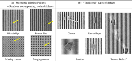
TSMC uses EUV double patterning because there are lots of features they need to pattern smaller than EUV’s minimal line width for 3 nm and below. Anything that requires 2 steps for EUV requires 4-6 steps with DUVi so no, no matter how much extra patterning you have to do with EUV you are saving a lot of steps relative to DUVi. The tradeoff is really over whether you can afford a feature to have higher line roughness, and whether the specific feature can be practically repaired after initial deposition and etching steps since that’s what the EUV stochastic noise issues are primarily affecting.

I dont think you have been following this thread. One the reason I said from a couple years that China has already has EUV machines is because all the ecosystem that has been develop around it. From EUV mask inspection tools, EUV metrology tools, to EUV photoresists, pellicle development and so on. None of that can happen in vacuum (no pun intended), my guess is that the EUV tooling and anchilliary ecosystem in China have is as advanced as whatever EUV lithography machine they have. The ecosystem is going neck to neck with the main tool.
One way to square the difference between our inferences and the claims here is that even if all the auxiliary ecosystem for a full EUV process is ready they all need some time to work out teething issues to reach a level of certification sufficient for mass deployment. You can use EUV for production and also not be confident enough with the process to deploy at scale. And if I had to guess that’s where I think we are at.
 
Last edited:

tokenanalyst

Brigadier
Registered Member
TSMC uses EUV double patterning because there are lots of features they need to pattern smaller than EUV’s minimal line width for 3 nm and below.
No, I think there is not 3nm width feature in 3nm process node, is just a marketing term to refer to a hypothetical equivalent 3nm planar transistor, For 3nm I think the gate length is like 13-18 nm and that is with double patterning because you need space to deal with LER errors due stochastics, so double patterning allows for breathing room and that is why Intel was pushing for High NA EUV so much because they didn't want to deal with multi-patterning because they never cultivated a good wafer processing strategy like TSMC and SMIC.

1754944387146.png
 

latenlazy

Brigadier
No, I think there is not 3nm width feature in 3nm process node, is just a marketing term to refer to a hypothetical equivalent 3nm planar transistor, For 3nm I think the gate length is like 13-18 nm and that is with double patterning because you need space to deal with LER errors due stochastics, so double patterning allows for breathing room and that is why Intel was pushing for High NA EUV so much because they didn't want to deal with multi-patterning because they never cultivated a good wafer processing strategy like TSMC and SMIC.

View attachment 157894
I didn’t mean to imply 3 nm line width with my comment. But even with 13.5 nm line width I imagine there are probably some patterning features that might fall below that line width, or at least a line width plus margin of error tolerance control requirement for factors like overlay accuracy. But yes, the higher stochastic errors are going to contribute to that tolerance control part of the equation as well, though I think it’s only added maybe 1-2 nm of additional error (which to be clear isn’t small for 13-18 nm features).

Either way the main point of the comment was any additional steps you take for EUV is still a multiple less than the number of steps trying to do the same pattern with DUVi, even with stochastic noise issues included.
 

tokenanalyst

Brigadier
Registered Member
I didn’t mean to imply 3 nm line width with my comment. But even with 13.5 nm line width I imagine there are probably some patterning features that might fall below that line width, or at least a line width plus margin of error tolerance control requirement for factors like overlay accuracy. But yes, the higher stochastic errors are going to contribute to that tolerance control part of the equation as well, though I think it’s only added maybe 1-2 nm of additional error (which to be clear isn’t small for 13-18 nm features).

Either way the main point of the comment was any additional steps you take for EUV is still a multiple less than the number of steps trying to do the same pattern with DUVi, even with stochastic noise issues included.
Ohh yeah, the problem is that EUV cost more, but if you have less patterning steps, like Intel wanted with HNA EUV so they could save wafer processing steps and in theory get better yields.
 

tokenanalyst

Brigadier
Registered Member

Another breakthrough in large-scale TGV technology: Sucos' fifth batch of equipment delivered leads the industry upgrade​


Sukos Semiconductor Equipment Technology Co., Ltd. recently delivered its fifth batch of TGV (through-glass via) electroplating equipment to customers after rigorous testing. This marks another important milestone for the company in the advanced packaging equipment field, following the successful shipment of the fourth batch of equipment. It also signifies that Sukos Semiconductor has reached industry-leading levels in both TGV equipment mass production capacity and technological maturity. TGV technology, at the core of advanced packaging, creates and metalizes through-holes in a glass substrate, achieving vertical electrical connections between the chip and the substrate.

Compared to traditional through-silicon via (TSV) technology, it offers significant advantages. Glass material has a low dielectric constant, which reduces signal loss and improves high-frequency transmission efficiency, making it suitable for high-end applications such as 5G and artificial intelligence. The glass substrate also offers excellent thermal stability and mechanical properties, remaining stable even at high temperatures. The low cost of glass and the simplified process reduce mass production costs, resulting in a more cost-effective solution. Therefore, it is considered a core direction for next-generation advanced packaging.

This fifth shipment of equipment utilizes Sucos' independently developed 510mm×515mm large-scale board-level technology, a leading industry specification with outstanding production efficiency. Compared to smaller substrates, large-scale board-level technology can integrate more chips, increasing output per unit time; improving material utilization, diluting equipment depreciation and energy costs; and optimizing wiring, shortening interconnect distances, and improving packaging density and performance. This meets the miniaturization and high-density requirements of next-generation devices, providing customers with a competitive advantage.​

Please, Log in or Register to view URLs content!
 

tokenanalyst

Brigadier
Registered Member

Characteristics of extreme ultraviolet emissions from interaction between delay-adjustable dual-wavelength laser and Sn target​


Abstract: Laser-produced plasma extreme ultraviolet (LPP-EUV) source is one of the key technologies in advanced lithography systems. Recently, solid-state lasers have been proposed as an alternative drive laser for the next-generation LPP-EUV source. Compared with currently used CO2 lasers, solid-state lasers have higher electrical-optical efficiency, more compact size, and better pulse shape tunability. Although limited to shorter operating wavelengths, the solid-state lasers have higher critical plasma density and optical depth. Consequently, re-absorption and spectral broadening cause lower conversion efficiency (CE). Therefore, to optimize EUV emission features and improve CE, a 0.532-μm pre-pulse laser is utilized in this work to modulate the plasma density distribution. The pre-pulse and a 1.064-μm Nd: YAG laser (the main pulse) are incident on an Sn slab target co-axially. The EUV energy and spectra of the Sn plasma are characterized at various delay times. It is demonstrated that compared with the 1.064-μm single pulse, the 0.532-μm pre-pulse laser with short delay times of 10 ns and 20 ns respectively results in a 4% increase in CE at 26° and 18% increase at 39°. The angular distribution of EUV energy is modulated by the 0.532-μm pre-pulse. An isotropic emission can be obtained within a certain delay time. The spectral feature near 13.5 nm is optimized, and a spectral purity of 12.2% is improved by 69%. The laser spot sizes of 0.3 mm and 1 mm for the pre-pulse are compared in the experiment. The results show that the 1-mm spot size has a better modulation effect on the EUV emission. Moreover, the time-resolved visible-band plasma profile is captured by an ICCD with 1.6-ns gate width. The plasma size and the distance to the target surface are increased by the 0.532-μm pre-pulse, which suggests that the energy of the main pulse is deposited in the low-density pre-plasma plume instead of in the plasma near the target surface. The lower plasma density leads to an increase in CE and spectral purity. The angular distribution of EUV energy is found to be closely related to the plasma morphology, and defined as the ratio of the longitudinal size to lateral size of the plasma. This indicates that the variation of plasma morphology can influence the angular distribution of EUV energy, which is caused by the 0.532-μm pre-pulse. This work has guiding significance for optimizing the emission characteristics of solid-state laser driven EUV sources.

Please, Log in or Register to view URLs content!
 

nativechicken

Junior Member
Registered Member
No, I think there is not 3nm width feature in 3nm process node, is just a marketing term to refer to a hypothetical equivalent 3nm planar transistor, For 3nm I think the gate length is like 13-18 nm and that is with double patterning because you need space to deal with LER errors due stochastics, so double patterning allows for breathing room and that is why Intel was pushing for High NA EUV so much because they didn't want to deal with multi-patterning because they never cultivated a good wafer processing strategy like TSMC and SMIC.

View attachment 157894
The source I mentioned also disclosed conclusions from China's highest-level closed-door briefings on this matter:

China has definitively established that the true measure of process advancement lies in transistor density, not mere gate pitch. This fundamental verdict was reached early on.

Facing critical shortages of advanced semiconductor equipment (ASML's DUVi new-order embargo since 2022/2023, not to mention earlier EUV restrictions—China’s last EUV purchase attempt involved acquiring 0.06% ASML shares in 2017, potentially worth hundreds of millions of euros, plus near-full prepayment for EUV tools, yet delivery still blocked in 2019), China immediately pivoted its strategy. Given transistor density’s primacy in chip performance, 3D stacking and advanced packaging emerged as essential pathways (increasing density vertically).

Thus, Huawei’s chip stacking solution fundamentally represents a predetermined technical trajectory formulated during China’s semiconductor industry’s highest-level strategy sessions.
 

latenlazy

Brigadier
The source I mentioned also disclosed conclusions from China's highest-level closed-door briefings on this matter:

China has definitively established that the true measure of process advancement lies in transistor density, not mere gate pitch. This fundamental verdict was reached early on.

Facing critical shortages of advanced semiconductor equipment (ASML's DUVi new-order embargo since 2022/2023, not to mention earlier EUV restrictions—China’s last EUV purchase attempt involved acquiring 0.06% ASML shares in 2017, potentially worth hundreds of millions of euros, plus near-full prepayment for EUV tools, yet delivery still blocked in 2019), China immediately pivoted its strategy. Given transistor density’s primacy in chip performance, 3D stacking and advanced packaging emerged as essential pathways (increasing density vertically).

Thus, Huawei’s chip stacking solution fundamentally represents a predetermined technical trajectory formulated during China’s semiconductor industry’s highest-level strategy sessions.

It’s not just transistor density. Transistor efficiency is also critically important, or thermal constraints prevent effective compute scaling. This is something Intel kept running into when it was trying to shrink below 10 nm. There’s been very clear investments toward improving transistor architecture designs (as well as the high precision etching and deposition tools needed to pursue this path) as part of China’s overall advanced node development strategy, and in fact without the ability to push faster cadence on node shrinks this is the most tractable path for achieving year over year iterative improvement, independent of packaging and stacking approaches.
 

leibowitz

Junior Member
I only joined this forum last year and haven't seen earlier posts.

But I've been aware of what you mentioned for some time—similar perspectives exist in China. The real question is: What’s the current resolution status? What’s today’s actual progress metric?

As an external observer, I consider this source exceptionally precise in characterizing China's semiconductor industrial status—concretely defining completion milestones versus remaining gaps (and where those gaps persist).

For instance, amid rampant EUV speculation, his detailed specification of one fact stands out: China achieved 5nm through extreme DUVi enhancements, not premature EUV adoption.

He acknowledged significant EUV breakthroughs but also underscored that the U.S. decisively severed China's EUV access in 2019, immediately enforcing comprehensive and effective embargoes across all EUV-related domains. Thus, expecting near-term EUV production deployment is unrealistic—there are foundational gaps to address first.

I can't vouch for his absolute accuracy, but his demonstrable work convinces me he engages regularly with China’s core semiconductor institutions/teams—though not at operational-level understanding. Crucially, his sourcing is highly credible, and he willingly clarifies technical principles in depth.

I don’t regard his technical expertise as superior to mine or others here. Yet his video revealed startling insights:

Mastery of cutting-edge semiconductor manufacturing workflows
Profound understanding of systemic challenges
Structured problem-solving frameworks
Having tracked microelectronics/semiconductor/lithography literature for over a decade, I grasp most core concepts. While perhaps less technically adept than many here, I'm far from credulous.

Countless domestic EUV/DUV claims surfaced recently—I remained silent, skeptical of all. But I trust his account. Why?

Not merely by revealing outcomes, but by:

➤ Exposing root constraints
➤ Detailing problem-solving frameworks
➤ Honestly stating: “We’re bottlenecked here—resolving this takes time”

Ultimately, that’s what ultimately builds credibility.
1. Who is this source?
2. Stop using AI to write your posts
 
Top