Chinese semiconductor thread II

tokenanalyst

Brigadier
Registered Member

High efficiency regulation method to generate an illumination source by adopting the micromirror array in DUV lithography​

Abstract​


Source and mask optimization (SMO) is an important lithography resolution enhancement technique for 22 nm technology nodes and beyond in lithography. This technique generates freeform sources by adjusting the inclination angle of the micromirror array (MMA). In this paper, a high efficiency regulation method to generate an illumination source by adopting the micromirror array in DUV lithography is proposed. The number and inclination angles of micromirrors required for adjustment to convert the initial source into any illumination source are quickly and accurately obtained by using the proposed method. The illumination source is obtained on the pupil plane by adjusting the inclination angles of some micromirrors. The simulation results show that the initial source is converted into another illumination source with different complexities by adjusting some micromirrors. Compared with the traditional MMA allocation method, when the initial source is the freeform source, the regulation efficiency of micromirrors has been improved by at least 20%. The method reduces the regulation time of micromirrors and the number of micromirrors required for adjustment. Moreover, the number of micromirrors required for adjustment is positively correlated with the coherence coefficient. The results illustrate that this method is effective and has significant engineering implications.

Please, Log in or Register to view URLs content!
 

tokenanalyst

Brigadier
Registered Member
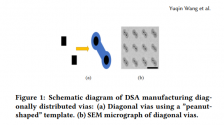
Less known method to achieve progress in the sub 7nm process node: DSA or Direct Self Assembly

An Automatic Insertion Scheme of Extra Via for DSA-MP Hybrid Lithography​

Abstract​

With the continuous shrinking of feature size, directed self-assembly (DSA) has gradually become one of the leading candidates for extending the resolution of optical lithography to sub-7 nm and beyond, a DSA-based extra via (EV) insertion scheme is the key to guarantee the reliability of integrated circuit when applying DSA during manufacturing. In this paper, we proposed an automatic insertion algorithm of extra via taking the manufacturing cost of the guiding template in DSA into consideration in the EV insertion process, which makes the total cost of subsequent DSA-MP hybrid lithography controllable, while maintaining a high insertion rate of EV. The simulation results show that, with the same experimental patterns, the insertion rate of EVs is increased by about 10% compared with the previous integer linear programming method.​

1728142904074.png

Please, Log in or Register to view URLs content!
 

Hyper

Junior Member
Registered Member
Less known method to achieve progress in the sub 7nm process node: DSA or Direct Self Assembly

An Automatic Insertion Scheme of Extra Via for DSA-MP Hybrid Lithography​

Abstract​

With the continuous shrinking of feature size, directed self-assembly (DSA) has gradually become one of the leading candidates for extending the resolution of optical lithography to sub-7 nm and beyond, a DSA-based extra via (EV) insertion scheme is the key to guarantee the reliability of integrated circuit when applying DSA during manufacturing. In this paper, we proposed an automatic insertion algorithm of extra via taking the manufacturing cost of the guiding template in DSA into consideration in the EV insertion process, which makes the total cost of subsequent DSA-MP hybrid lithography controllable, while maintaining a high insertion rate of EV. The simulation results show that, with the same experimental patterns, the insertion rate of EVs is increased by about 10% compared with the previous integer linear programming method.​

View attachment 136941

Please, Log in or Register to view URLs content!
DSA can't be used for patterning, only pattern correction.
 

tokenanalyst

Brigadier
Registered Member
DSA can't be used for patterning, only pattern correction.
I think you maybe confusing Self-Alignment with DSA (Direct Self-Assembly). Along with EUV and NIL is one of the future patterning technique for node shrinking, It could allow current DUV tools to extent into more denser process nodes.


gotodistance

New Member
Registered Member
Innovation!! China's new breakthrough first!! Optoelectronic chips == Electric vehicles: "Silicon photonics", or optoelectronic chips, will create a new semiconductor ecosystem like China's electric vehicles. Optoelectronic chips do not require EUV.
China's state-run semiconductor research institute JFS Research Institute said it has achieved a "milestone" in the development of silicon photonics, which it said could help China overcome technical barriers to current chip design and achieve self-sufficiency amid US sanctions.

Innovation!! China's new breakthrough second!! Chinese startup Numemory claims memory chip innovation amid US technology sanctions: SCM is a memory and storage technology that combines the features of dynamic random access memory (DRAM) found in smartphones and other consumer electronics with those found in conventional NAND flash storage. Sometimes called persistent memory, SCM provides fast, non-volatile memory for processors used in servers and storage systems in data centers. It said that SSDs made with SCM technology could provide data centers and cloud computing service providers with large capacity, high density, high bandwidth, and low latency storage solutions.

Please, Log in or Register to view URLs content!
 
Top