Chinese semiconductor thread II

GulfLander

Senior Member
Registered Member
"Foxconn is building the world's largest Nvidia GB200 chip manufacturing facility to help meet "awfully huge" demand for the AI darling's Blackwell platform, a senior executive at the Taiwanese company said on Tuesday."

GZVgdUbW8AAQkpR.png

Please, Log in or Register to view URLs content!
 

gelgoog

Lieutenant General
Registered Member
I posted a link at bottom of post # 4923, from piq...
PiQ is an aggregator, not the source article, and I get redirected to a different page when I click on that link, and cannot access the article from there. I literally had to search for the original article by typing the name of the article as in the embedded image you had in the post.
 

tokenanalyst

Brigadier
Registered Member

Wuhan University of Science and Technology team makes rice grow semiconductor materials​


China Education News - China Education News Network (Reporter Cheng Mo, Correspondent Zou Yifan) On October 8, the reporter learned from Wuhan University of Science and Technology that the "Jointly Working with Rice" student team of the School of Materials of the university used low-temperature magnesium thermal technology to extract and produce a semiconductor material - nano-silicon carbide from rice straw and rice husks. The particle size can be as fine as 30nm and the purity can reach 99.99%, increasing the added value of rice husks by more than 9 times.

Rice contains agricultural byproducts such as rice straw and rice husk. my country produces hundreds of millions of tons of agricultural byproducts similar to rice every year. Traditional incineration seriously pollutes the environment. Now it is often used as feed and bioenergy, with little profit and low added value.

Wei Yiqi, the team leader, has been studying silicon carbide since 2021. He led team members to conduct research in rural areas across the country and found that agricultural by-products were seriously accumulated and the comprehensive utilization rate was less than 50%. After testing more than 30 kinds of agricultural by-products, it was found that rice has a high silicon oxide content and a uniform particle size.

How to synthesize nano-silicon carbide on a large scale from agricultural byproducts such as rice straw and rice husk at low temperature and conveniently, and control its size and shape is a technical difficulty. The carbon thermal reduction method commonly used in domestic and foreign industries has a temperature of 1600~2200℃, high energy consumption, low purity, and complex conversion process.

Through experiments and thermodynamic calculations, the team optimized the process parameters after hundreds of attempts, and transformed the natural nano-silicon oxide in rice straw and rice husk into uniform nano-silicon carbide products by reacting carbon. During the reaction, the team developed low-temperature magnesium thermal technology and dynamic heat control technology, which broke through the nano-silicon carbide sintering problem caused by local high temperature in the magnesium thermal process, ensuring small and uniform particle size.

Wei Yiqi introduced that the team had carried out pilot work in rural areas, purchasing rice husks from farmers at a price 100% higher than the market price, and using low-temperature technology to produce high-purity nano-silicon carbide products, which can increase the company's turnover by more than 10 million yuan in three years. The current project has completed the pilot stage and is conducting strategic cooperation with enterprises to conduct product trials. The team plans to establish agricultural by-product raw material processing bases in various villages and towns to help farmers increase their income.

Professor Gu Huazhi, executive director of the State Key Laboratory of Refractories and Metallurgy at Wuhan University of Science and Technology, praised the achievement: "It has achieved high added value utilization of agricultural by-products, increased farmers' income, and explored a new way for science and technology to help rural revitalization."

Nano-silicon carbide can be used in chip manufacturing, high-end ceramics, etc., and the global silicon carbide production is in short supply. Wei Yiqi said: "We will also iterate the technology and plan to develop a complete nano-silicon carbide conversion technology to utilize other agricultural by-products, help develop green agriculture, and become a practitioner of rural revitalization!"​

Please, Log in or Register to view URLs content!
 

tokenanalyst

Brigadier
Registered Member
Yuntian Semiconductor: Glass substrate wafer-level products are first launched

The fan-out packaging based on glass substrates is progressing very fast. Although the panel-level glass substrate based on through-glass vias is in full swing and advancing rapidly, global industrialization has not yet really begun. For the actual commercialization and large-scale application of glass-based products, glass wafer-level packaging is currently at the forefront.

As the first manufacturer in China to realize mass production of glass wafer-level packaging, Xiamen Yuntian Semiconductor Co., Ltd. takes the innovation of microsystem integration technology and the promotion of the development of the semiconductor industry as its mission. In terms of technical products, Xiamen Yuntian Semiconductor focuses on 5G RF, IoT, power devices, AI (CPU/GPU), biomedicine, and emerging application fields. It currently has more than 100 customers, including more than 20 key customers from leading companies. In advanced packaging, it has achieved the industrialization of 4/6/8/12-inch wafer-level 3D packaging, fan-out packaging, and 2.5D glass 3D packaging, and has made great progress in RF filter 3D packaging, power device metallization, integrated passive devices, inductors/capacitors/resistors, filters/antennas.

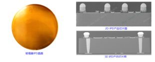
In the field of glass through-holes and devices, Yuntian Semiconductor has taken the lead in developing IPD integration technology based on glass substrates, including a series of IPD devices such as capacitors, inductors and passive filters. In terms of glass-based inductors, at 0402 size and 1GHZ frequency, samples with an inductance of 13.57nH and a Q value of 53.93 can be prepared. At 500MHZ frequency, the overall inductance is 1.58~13.03nH, and the Q value is 30.93~43.22nH. In terms of TGV-based DTC technology, a low-cost DTC process is developed, with a glass-based array blind groove structure with an opening of 15 µm, a depth of 250 µm, and a width of 250 µm. ALD and CVD are used to prepare capacitor metal-insulator-metal stacks to obtain a DTC capacitance density of 68 nf/mm².
1728397226383.png
1728397244284.png

Please, Log in or Register to view URLs content!
 

tokenanalyst

Brigadier
Registered Member

SIRUI Intelligent's dual-line business layout helps China's semiconductor equipment localization technology innovation.​


At the CSEAC 2024 main summit forum,the chairman of SRI Intelligent, reported on the company's latest progress: "Since its release at the CSEAC conference last year, SRI Intelligent's high-energy ion implanter has been successfully moved to the client and started process verification. With the strong support of customers, the equipment has been successfully transferred to the mass production stage in the first half of this year, the key technical indicators have been fully verified, and the equipment replacement rate has reached a satisfactory level. In addition, in the past year, the SRII high-energy ion implanter has also completed a large number of tests for logic, storage and power device customers, all of which can meet the needs of different applications, and is expected to be used in more fields this year."

As Chairman Nie Xiang summarized, after three years of unremitting efforts, SIRUI Intelligent has built a series of platform-based ion implanter product lines, based on high-energy ion implanters and large-beam ion implanters, and continuously expanded to cover power semiconductor fields including silicon carbide (SiC) to meet diverse application needs. This series of technological advances not only marks that SIRUI Intelligent has made a major breakthrough in the field of ion implantation technology, but also indicates that the competitiveness of domestic ion implanters in the international market is gradually increasing.

1728398912481.png

Focusing on ALD to create key equipment for third-generation semiconductor manufacturing

While ion implantation technology continues to make breakthroughs, SIRUI Intelligence has also continued to work hard on atomic layer deposition (ALD), a business with more than 40 years of technology accumulation. At the Power and Compound Semiconductor Industry Development Forum held during the exhibition, Chen Xianglong, deputy general manager of SIRUI Intelligence, focused on how to choose the right thin film deposition equipment to match the evolving wide bandgap semiconductor manufacturing process requirements as third-generation semiconductor materials such as silicon carbide (SiC) and gallium nitride (GaN) show great potential in high temperature, high pressure and high frequency applications.

1728398955221.png

Please, Log in or Register to view URLs content!
 

tokenanalyst

Brigadier
Registered Member

Iodonium functionalized polystyrene as non-chemically amplified resists for electron beam and extreme ultraviolet lithography​

Key Laboratory of Photochemical Conversion and Optoelectronic Materials, Technical Institute of Physics and Chemistry, University of Chinese Academy of Sciences

Abstract​

A novel non-chemically amplified resist (n-CAR) based on biphenyl iodonium perfluoro-1-butanesulfonate-modified polystyrene with a naphthalimide scaffold (PSNA0.4) was synthesized and characterized. Through extensive exploration using dose-dependent resist thickness analysis, acetonitrile was identified as the optimal developer. Employing electron beam lithography (EBL), the n-CAR of PSNA0.4 demonstrated its high-resolution patterning capability by resolving a dense line pattern of 18 nm L/S at an exposure dose of 1300 μC cm−2, achieving a high contrast of 7.1. Further studies using extreme ultraviolet lithography (EUVL) demonstrated that the PSNA0.4 resist can achieve 22 nm L/S patterns at a dose of 90.8 mJ cm−2, underscoring its high sensitivity for n-CARs. Detailed studies to gain insights into the underlying patterning mechanisms using X-ray photoelectron spectroscopy (XPS) suggest that the cleavage of polar iodonium into nonpolar polystyrene (PS)-based iodobenzene species enables a solubility switch, resulting in negative lithographic patterns. These findings highlight the innovative potential of the PSNA0.4 resist in advancing the capabilities of n-CAR technologies, particularly in the realms of EBL and EUVL, for high-resolution lithographic applications.

1728399638498.png
1728399663313.png

Please, Log in or Register to view URLs content!
 
Top