Chinese semiconductor thread II

Phead128

Captain
Staff member
Moderator - World Affairs
What total annihilation looks like.

Please, Log in or Register to view URLs content!
The article is so disingenuous, it admits in half-way that reduced revenue is mostly due to year-end seasonality and only "slight" quarterly decline in revenue. Yet it makes the huge logical leap to reduced profits (presumably implying yields) with zero evidence whatsoever. Pure conjecture and speculation. They really are scrapping the bottom for barrel in journalism these days.

But to your broader point, oh how far the goalpost has shifted from dead to "slightly less profitable". SMIC still profitable (unlike Intel), yet they spin it as a loss.
 

Blitzo

Lieutenant General
Staff member
Super Moderator
Registered Member
Please, Log in or Register to view URLs content!

Maybe the new phone in November won't come with a 5nm chip.

What does the actual full article say? If the article that Siege posted above (#4779) is quoting the digitimes article accurately as stated, it seems there doesn't seem to be any remark about the status of whether the new phone will have a 5nm process or not.

If the original article behind the pay wall says something specifically about 5nm, then that's another matter.
 

tphuang

Lieutenant General
Staff member
Super Moderator
VIP Professional
Registered Member
Please, Log in or Register to view URLs content!

Huawei has helped China Mobile build a large AI data center in Harbin with 18000 card Ascend cluster providing 6.9 EFLOPS of computation. Not sure why the average computation per card in there is greater than 320 TFLOPS. Maybe they already have some Ascend-910C in there.

This data center is 100% domestic supplied.
 

tphuang

Lieutenant General
Staff member
Super Moderator
VIP Professional
Registered Member
Please, Log in or Register to view URLs content!

Looks like the Dutch Govt is between those who are more pro-restriction vs less restriction toward Chinese export.

I also get the feeling that ASML is really telling Dutch gov't they are losing sales in China due to the restrictions already put in place.
 

tokenanalyst

Brigadier
Registered Member

Xingfu Electronics breaks the "bottleneck" situation of wet electronic chemicals and helps improve the security of the domestic semiconductor supply chain.​


As a company with core technological competitiveness, Xingfu Electronics is well aware of the importance of mastering key core materials and technologies. Since its inception, it has continued to increase its R&D investment, insist on independent technological innovation, accelerate the solution of "bottleneck" problems, and gradually achieve domestic substitution of wet electronic chemicals.

From 2021 to 2023, Xingfu Electronics' R&D expenses were RMB 25.8319 million, RMB 53.0594 million, and RMB 56.7608 million, respectively. The continuous increase in the amount of R&D expenses not only demonstrates the company's emphasis on technological innovation, but also lays a solid foundation for its technological breakthroughs in core products such as electronic-grade phosphoric acid, electronic-grade sulfuric acid, and etching solution.

With high R&D investment, Xingfu Electronics' core technologies have achieved continuous breakthroughs. In 2013, the company's electronic-grade phosphoric acid products reached the highest level G3 of the SEMI electronic-grade phosphoric acid product standard; in 2017, the company's electronic-grade sulfuric acid products achieved a breakthrough in the SEMI standard G4 level for wet electronic chemicals; in 2020, the company's electronic-grade sulfuric acid products achieved a breakthrough in the SEMI standard G5 level for wet electronic chemicals; in November 2022, the company's electronic-grade phosphoric acid and electronic-grade sulfuric acid related technologies were appraised by an expert group organized by the China Electronic Materials Industry Association, and the appraisal conclusion was that the company's overall technology of electronic-grade phosphoric acid and electronic-grade sulfuric acid has reached the international advanced level.

1727360482998.png


At present, Xingfu Electronics has achieved key technological achievements such as the key technology of preparing high-purity yellow phosphorus by step-by-step purification of industrial yellow phosphorus, the key technology of producing electronic-grade sulfuric acid by gas purification absorption method, and the key technology of formulating high-performance electronic-grade mixed chemicals. As of June 30, 2024, the company has obtained 116 patent authorizations, including 77 invention patents, 37 utility model patents, and 2 design patents.

At present, the electronic-grade phosphoric acid, electronic-grade sulfuric acid and other general wet electronic chemicals produced by Xingfu Electronics have been widely used in leading companies in the industry. Customers include TSMC, SK Hynix, SMIC, Yangtze Memory Technologies, Huahong Group, Changxin Memory Technologies, Xinlian Integration, Globalfoundries, UMC, Texas Instruments (Chengdu), CanSemi, China Resources Shanghua, Wuhan Xinxin, Jinghe Integration, BYD Semiconductor, Xin'en Integration, Chongqing Wanguo, Yandong Microelectronics, Entegris, CMC Materials, Silterra and other well-known domestic and foreign integrated circuit industry companies. It can provide a stable supply of 8-inch and 12-inch wafer manufacturing for the integrated circuit industry, suitable for advanced processes of 28nm and below.

Please, Log in or Register to view URLs content!
 

tokenanalyst

Brigadier
Registered Member

Domestically developed 28nm display chips are put into mass production​


According to Beijing Yizhuang, the world's first 28nm embedded RRAM (resistive random access memory) picture quality adjustment chip developed by Chinese semiconductor manufacturer Xianxin Technology Co., Ltd. (hereinafter referred to as "Xianxin Technology") and domestic research institutes has been officially mass-produced in Beijing and successfully applied to the Mini LED (sub-millimeter light-emitting diode) high-end series TVs of domestic leading customers.

Yan Chenghui, general manager and founder of DisplayCore Technology, said that the world's top semiconductor technology has reached the 2nm era, but for semiconductor displays, 28nm is the ceiling of domestic technology, considering the cost. Among them, the image quality adjustment chip requires the integration of various compensation algorithms, which is difficult to develop and requires advanced logic processes for manufacturing. It is one of the products with the lowest localization rate in the display chip category.

Please, Log in or Register to view URLs content!
 

tokenanalyst

Brigadier
Registered Member

The first in China! Photonic chip pilot line is put into use in Wuxi​


Wuxi has made another major move in promoting the technological research and application of quantum technology, a future industry, throughout the entire chain. On the 25th, the first photonic chip pilot line in China built by the Wuxi Photonic Chip Research Institute of Shanghai Jiaotong University was officially put into use. This marks that photonic chips have officially entered the fast lane of industrialization, which will break through the limitations of the original computing paradigm and bring new imagination space for large-scale intelligent computing.

the total area of the pilot platform is 17,000 square meters. It integrates scientific research, production and services, covering the entire closed-loop process of thin-film lithium niobate photonic chips from lithography, thin-film deposition, etching, wet process, cutting, measurement to packaging. It can not only provide full-process technical services for universities, research institutes and innovative enterprises, but also provide photonic industry incubation projects, efficiently link with industrial funds, open up the complete chain from product research and development to marketization, and accelerate the commercialization of scientific and technological achievements.​

1727361193836.png1727361217352.png

Please, Log in or Register to view URLs content!
 

huemens

Junior Member
Registered Member
What does the actual full article say? If the article that Siege posted above (#4779) is quoting the digitimes article accurately as stated, it seems there doesn't seem to be any remark about the status of whether the new phone will have a 5nm process or not.

If the original article behind the pay wall says something specifically about 5nm, then that's another matter.

He didn't say anything about 5nm or even anything about the next phone. A week ago there was a Huawei event where he gave a speech about AI in China. Mostly about Huawei's advancements in that area, the challenges and how Huawei is trying to overcome those challenges. In the bit they are quoting what he basically said was China currently does not have have access to the most leading-edge process node (obviously), so we have to make do with whatever node is available and Huawei is innovating in other ways to compensate for that. I don't have the DigiTimes article but all other articles this week with similar titles are taken from this bit in the speech.
Computing power largely depends on semiconductor manufacturing process nodes. However, the reality is that US restrictions on AI chips for China are unlikely to be lifted anytime soon, and the Chinese mainland will lag behind in semiconductor manufacturing process nodes for a relatively long time. This undermines our ability to make advanced chips. It's a challenge that we have to confront when developing computing solutions. In the Chinese mainland, sustainable computing power can only be achieved with chip manufacturing process nodes that are practically available.

These challenges are real, but they also present opportunities and new possibilities. They are what motivate us to keep innovating. AI is becoming the predominant source of demand for computing power – and this trend is driving structural changes in computing systems. We're now looking at how to increase computing power at the system level rather than the individual processor level.
These structural changes give us the opportunity to create a new computing architecture – a viable path for the independent and sustainable development of the computing industry.

We want to seize the opportunities presented by this AI revolution based on chip manufacturing process nodes that are practically available. And so, our strategy is to create a new computing architecture that is built on synergistic innovation across computing, data storage, and networks. We will also develop computing supernodes and clusters to sustainably meet long-term demand for computing power.

Full text of the speech:
Please, Log in or Register to view URLs content!
 
Last edited:

tokenanalyst

Brigadier
Registered Member

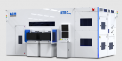
ACM Shanghai launches Ultra C bev-p panel-level edge etching tool​


ACM Semiconductor Equipment Co., Ltd. (hereinafter referred to as “ACM Shanghai”) a leading supplier of wafer process solutions for semiconductor front-end and advanced wafer-level packaging applications, today launched its new Ultra C bev-p panel edge etch tool for fan-out panel-level packaging (FOPLP) applications.

The equipment is specially designed for edge etching and cleaning in copper-related processes. It can handle edge etching on the front and back sides of the panel at the same time, significantly improving process efficiency and product reliability.

Dr. Hui Wang, Chairman of ACM Shanghai, said: We see the growing importance of fan-out panel-level packaging as the technology meets the evolving needs of modern electronic applications with advantages in integration density, cost efficiency and design flexibility. Thanks to our deep expertise in wet processes, ACM Shanghai’s new Ultra C bev-p tool is one of the first double-sided edge etch tools available for panel-level applications. Together with our Ultra ECP ap-p panel-level horizontal plating tool and Ultra C vac-p negative pressure cleaning tool launched this year, we expect the Ultra C bev-p to advance the industry of large panel advanced packaging with high-precision features and the market for fan-out panel-level packaging technology.”

The Ultra C bev-p equipment uses a wet etch process designed for edge etching and copper residue removal, which plays a vital role in fan-out panel-level packaging technology. This process is critical to effectively avoid electrical shorts, minimize the risk of contamination, and maintain the integrity of subsequent process steps, helping to ensure the durability of the device. The efficiency of this equipment is mainly due to ACM Shanghai's patented technology to meet the unique challenges posed by square panel substrates.

Unlike traditional round wafers, ACM Shanghai's unique design enables precise edge removal, ensuring that processing on warped panels is limited to the edge area. This patented technology is critical to maintaining the integrity of the etching process and delivering the high performance and reliability required for advanced semiconductor technology.

Designed for panel substrates, the Ultra C bev-p is compatible with organic, glass and bonded panels. The Ultra C bev-p can effectively manage the front and back sides of panels ranging from 510mm x 515mm to 600mm x 600mm, with thicknesses ranging from 0.5mm to 3mm. The equipment can handle warpage up to 10mm, ensuring optimal process conditions.
· Advanced panel handling: The Ultra C bev-p is equipped with automatic operation devices to ensure safe and precise handling and transfer of panels.
· Highly efficient copper removal: Ultra C bev-p uses dilute sulfuric acid and peroxide (DSP), a combination of deionized water, sulfuric acid and hydrogen peroxide, to effectively remove copper. In addition, the equipment uses deionized water for rinsing and N2 for final drying to ensure a clean and dry surface.
High throughput: The Ultra C bev-p is capable of running up to six chambers and processing 40 panels per hour (PPH), enabling high-efficiency mass production.
The system has an edge control accuracy of ±0.2mm and a control range of 0-20mm. With a mean time between failures (MTBF) of 500 hours and an uptime of 95%, it provides excellent reliability, stable performance and high operational efficiency.
1727362319395.png

Please, Log in or Register to view URLs content!
 

tphuang

Lieutenant General
Staff member
Super Moderator
VIP Professional
Registered Member

Domestically developed 28nm display chips are put into mass production​


According to Beijing Yizhuang, the world's first 28nm embedded RRAM (resistive random access memory) picture quality adjustment chip developed by Chinese semiconductor manufacturer Xianxin Technology Co., Ltd. (hereinafter referred to as "Xianxin Technology") and domestic research institutes has been officially mass-produced in Beijing and successfully applied to the Mini LED (sub-millimeter light-emitting diode) high-end series TVs of domestic leading customers.

Yan Chenghui, general manager and founder of DisplayCore Technology, said that the world's top semiconductor technology has reached the 2nm era, but for semiconductor displays, 28nm is the ceiling of domestic technology, considering the cost. Among them, the image quality adjustment chip requires the integration of various compensation algorithms, which is difficult to develop and requires advanced logic processes for manufacturing. It is one of the products with the lowest localization rate in the display chip category.

Please, Log in or Register to view URLs content!
Looks like 显芯科技 is a chip design firm. And if it is being mass produced in Beijing, then I think this is most likely Jingcheng fab. Actually pretty good indication of domestic fab and chip designer firm now picking up orders as a result of supply chain security.
 
Top