right, that's the difference between the two. CXMT has been a huge buyer of Western equipment this year, because they are still able to do so. My understanding is that the new tools are for 18.6nm DRAMs. The more cutting edge stuff they are doing like D1z and LPDDR5 still has to be done in their older fab.YMTC is also ramping up their facility and they don't mind supplying Huawei. But then again YMTC was put in the Entity List and CXMT is still not in it I think.
You are using an out of date browser. It may not display this or other websites correctly.
You should upgrade or use an alternative browser.
You should upgrade or use an alternative browser.
Chinese semiconductor thread II
- Thread starter vincent
- Start date
Puretech Semiconductor Cleaning Project Settles in Zhuhai High-tech Zone
At the ceremony, Zhuhai High-tech Zone signed a strategic cooperation agreement with Shanghai Zhichun Clean System Technology Co., Ltd. (hereinafter referred to as "Zhichun Technology"). Tan Chun, member of the Standing Committee of Zhuhai Municipal Party Committee and member of the Party Leadership Group of the Municipal Government, Zhang Ge, Deputy Director of the Economic Development Bureau of Hengqin Guangdong-Macao Deep Cooperation Zone, Xue Fei, member of the Party Working Committee of Zhuhai High-tech Zone and Deputy Director of the Management Committee, Jiang Yuan, Chairman of Zhichun Technology, and Chen Wei, Chairman of Guangdong Integrated Circuit Industry Association, attended the event.
The semiconductor cleaning project of Zhichun Technology signed this time was introduced through the joint cooperation of Zhuhai High-tech Zone and Hengqin Guangdong-Macao Deep Cooperation Zone. A large-scale semiconductor cleaning factory will be built in Zhuhai High-tech Zone to drive all product lines to expand into the South China market.
After completion, the project will be able to provide "2-hour supporting circle" services for semiconductor wafer factories in the Pearl River Delta. After the full business is put into operation, the annual output value will be no less than 1.2 billion yuan, which will inject new vitality into the development of Zhuhai's integrated circuit and semiconductor industry cluster and improve the semiconductor and integrated circuit industry chain.
AMEC speeding the research of cryogenic etching to compete with LAM and TEL in 3DNAND
CCP: As of 24H1, the company has produced and shipped more than 3,600 CCP etching reactors, and the number of newly shipped equipment in 24H1 has reached a record high; among them, the new shipments of Primo D-RIE/AD-RIE/AD-RIE-e in the dual reactor in 24H1 exceeded the full-year shipments in 2023, and the single reactor Primo HD-RIE/HD-RIEe/UD-RIE24H1 shipments increased by about 3 times compared with the full-year shipments in 2023. Primo AD-RIE-e continues to be shipped for the most advanced logic chip production lines, and has obtained repeat orders for advanced storage production lines. Primo SD-RIE has entered the yield test stage for the verification of the metal mask integrated Damascus etching process at the first advanced logic client, and has entered the second customer for on-site verification; and has reached evaluation intentions with many customers, and the current laboratory development is progressing smoothly. Primo UD-RIE has verified the mass production capability of etching ≥60:1 aspect ratio structures on the production line.
In addition, the company actively deploys ultra-low temperature etching technology, invests a lot of resources in the research of ultra-low temperature electrostatic chucks and new etching gases, and actively reserves cutting-edge technologies for etching higher aspect ratio structures (≥90:1).
ICP: The verification of multiple ICP devices in advanced logic chips, advanced DRAM and 3D NAND production lines has been progressing smoothly and has successively obtained bulk orders from customers. Nanova VE HP has invested in large-scale production in the application of high aspect ratio polysilicon masks in DRAM manufacturing. LUX has gradually achieved small-scale production on the production lines of multiple customers. PrimoTwinStar has achieved mass production on the production lines of mature logic chips, Meta Lens for AR glasses and other special devices for domestic and foreign customers, and has obtained repeat orders. The first Primo-Twin Star 200 was also delivered to the client for Meta Lens production line certification. While Primo TSV 200E/300E continues to receive repeat orders in mature markets, it has been successfully verified in the silicon via etching process of 12-inch 3D chips and has the opportunity to obtain certification on the world's first 12-inch MEMS chip production line newly built by European customers. The wafer edge Bevel etching equipment has been completed and is about to enter customer verification.
Thin film deposition equipment: The company's tungsten series of thin film deposition products can cover all tungsten applications of storage devices, and has completed the verification of CVD/HAR/ALD W tungsten equipment by multiple logic and storage customers, and has obtained customer orders. The EPI equipment R&D team has formed independent intellectual property rights and innovative pre-treatment and epitaxial reaction chamber design solutions; currently, the EPI equipment has successfully entered the customer verification stage. In 24H1, the company's new LPCVD equipment achieved its first sale, with revenue of 28 million yuan; LPCVD received new orders of 168 million yuan.
CXMT bought IP from Qimonda. YMTC developed it by itself. Might say something about the organisation.right, that's the difference between the two. CXMT has been a huge buyer of Western equipment this year, because they are still able to do so. My understanding is that the new tools are for 18.6nm DRAMs. The more cutting edge stuff they are doing like D1z and LPDDR5 still has to be done in their older fab.
apparently, CXMT got a lot better under the current bossCXMT bought IP from Qimonda. YMTC developed it by itself. Might say something about the organisation.
so they are going from 60:1 to 90:1.
AMEC speeding the research of cryogenic etching to compete with LAM and TEL in 3DNAND
CCP: As of 24H1, the company has produced and shipped more than 3,600 CCP etching reactors, and the number of newly shipped equipment in 24H1 has reached a record high; among them, the new shipments of Primo D-RIE/AD-RIE/AD-RIE-e in the dual reactor in 24H1 exceeded the full-year shipments in 2023, and the single reactor Primo HD-RIE/HD-RIEe/UD-RIE24H1 shipments increased by about 3 times compared with the full-year shipments in 2023. Primo AD-RIE-e continues to be shipped for the most advanced logic chip production lines, and has obtained repeat orders for advanced storage production lines. Primo SD-RIE has entered the yield test stage for the verification of the metal mask integrated Damascus etching process at the first advanced logic client, and has entered the second customer for on-site verification; and has reached evaluation intentions with many customers, and the current laboratory development is progressing smoothly. Primo UD-RIE has verified the mass production capability of etching ≥60:1 aspect ratio structures on the production line.
In addition, the company actively deploys ultra-low temperature etching technology, invests a lot of resources in the research of ultra-low temperature electrostatic chucks and new etching gases, and actively reserves cutting-edge technologies for etching higher aspect ratio structures (≥90:1).
ICP: The verification of multiple ICP devices in advanced logic chips, advanced DRAM and 3D NAND production lines has been progressing smoothly and has successively obtained bulk orders from customers. Nanova VE HP has invested in large-scale production in the application of high aspect ratio polysilicon masks in DRAM manufacturing. LUX has gradually achieved small-scale production on the production lines of multiple customers. PrimoTwinStar has achieved mass production on the production lines of mature logic chips, Meta Lens for AR glasses and other special devices for domestic and foreign customers, and has obtained repeat orders. The first Primo-Twin Star 200 was also delivered to the client for Meta Lens production line certification. While Primo TSV 200E/300E continues to receive repeat orders in mature markets, it has been successfully verified in the silicon via etching process of 12-inch 3D chips and has the opportunity to obtain certification on the world's first 12-inch MEMS chip production line newly built by European customers. The wafer edge Bevel etching equipment has been completed and is about to enter customer verification.
Thin film deposition equipment: The company's tungsten series of thin film deposition products can cover all tungsten applications of storage devices, and has completed the verification of CVD/HAR/ALD W tungsten equipment by multiple logic and storage customers, and has obtained customer orders. The EPI equipment R&D team has formed independent intellectual property rights and innovative pre-treatment and epitaxial reaction chamber design solutions; currently, the EPI equipment has successfully entered the customer verification stage. In 24H1, the company's new LPCVD equipment achieved its first sale, with revenue of 28 million yuan; LPCVD received new orders of 168 million yuan.
If 60:1 is sufficient for 160 layers, then 90:1 should be sufficient for 232 layers.
Very interesting video. There are three presentations in it
First one talk about computational lithography
Second one talk about EBL(e-beam lithography). It says that the gap between Chinese domestic EBL and leading international player,is much larger than that of scanner lithography(DUV/EUV etc). They are currently developing software for EBL,and it is in cooperation with Huawei CETC etc
Third one talk about metrology&inspection. It mentioned a case that a fab have detect certain wafer defects with their machine,but the the other ASML IRIS machine also in that fab failed to detect it
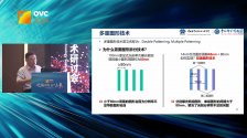
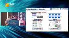
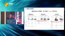
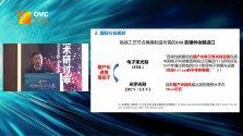
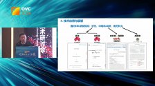
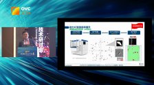


so they confirmed the 28nm machines?Very interesting video. There are three presentations in it
First one talk about computational lithography
Second one talk about EBL(e-beam lithography). It says that the gap between Chinese domestic EBL and leading international player,is much larger than that of scanner lithography(DUV/EUV etc). They are currently developing software for EBL,and it is in cooperation with Huawei CETC etc
Third one talk about metrology&inspection. It mentioned a case that a fab have detect certain wafer defects with their machine,but the the other ASML IRIS machine also in that fab failed to detect it
View attachment 136366
View attachment 136367
View attachment 136368
View attachment 136369
View attachment 136370
View attachment 136371
View attachment 136372
In addition, the company actively deploys ultra-low temperature etching technology, invests a lot of resources in the research of ultra-low temperature electrostatic chucks and new etching gases, and actively reserves cutting-edge technologies for etching higher aspect ratio structures (≥90:1).
Cryogenic etching is an that re-emerged recently.
This is how I have understood it (I'm not an expert): In reactive ion etching, surface to etch is attacked by shooting ions at it, like in a sandblast, and also by chemical reactions with the aforementioned ions. Shooting ions is very an-isotropic, i.e. you etch mostly in one direction (the one you shoot ions to), chemical reaction occurs instead all over the place.
To etch a narrow and deep hole you want your etching to be very anisotropic: attack only the surface at the bottom of the hole, while leaving sidewalls intact. To do this you want to reduce the ion's chemical reaction speed. In cryogenic etching you achieve this by cooling the wafer at below -100 Celsius, so that chemical reactions are greatly slowed down (speed of chemical reaction depends on temperature) and hence sidewalls are better preserved.
Lam Research re-introduced cryogenic etching in 2019 and now they are .
Tokyo Electron (TEL) presented their solution .
In both cases they claim that with cryo-etching it will be possible to reach 400 layers and beyond!
So this is a technology for the future, with good scalability for years to come.
Now also AMEC says that they are developing such a technology, currently they have a 5 years gap with LAM and about 1 with TEL, but hopefully they will able to close the gap much sooner...
apparently, CXMT got a lot better under the current boss
so they are going from 60:1 to 90:1.
If 60:1 is sufficient for 160 layers, then 90:1 should be sufficient for 232 layers.
If cryo-etching is needed only for aspect ratio structures (≥90:1) and they reached 160 layers with 60:1, apparently they can reach 232 layers without cryo-etching: that would be a big relief, this gives them about another 2 years to develop the technology.
Last edited:
