Chinese semiconductor thread II

tokenanalyst

Brigadier
Registered Member


The Tongfutongda advanced packaging and testing base project with an investment of 7.5 billion yuan has started, including board-level packaging!​


The Tongfu Advanced Packaging and Testing Production Base Project is a major provincial project in 2024, including two sub-projects, Tongfu Tongda and Tongfu Tongke. The Tongfu Tongda project mainly covers integrated circuit packaging products such as 5G, memory, flip-chip and wafer-level packaging, and has obtained a pile foundation construction permit. The Tongfu Tongke project rents a standard factory building in the Science and Industrial Park of Shibei High-tech Zone and builds a new comprehensive factory building of about 5,000 square meters, investing more than 4,000 sets of packaging and testing equipment. The investor, Tongfu Microelectronics Co., Ltd., is a national key high-tech enterprise specializing in advanced packaging and testing of integrated circuits, and is the second largest integrated circuit packaging and testing company in China. After the project is completed, it will greatly expand the advanced packaging and testing capacity, and further promote the development of Nantong's integrated circuit industry to a new level.

It is reported that Nantong has a good foundation for the integrated circuit industry, and has initially formed a full industrial chain with packaging and testing as the main body, extending to design, manufacturing, equipment and materials, etc., gathering a number of well-known companies such as Tongfu Microelectronics, and the overall scale ranks fourth in the province. In 2023, the city will have 67 enterprises above designated size, with an output value of 32.99 billion yuan.​

Please, Log in or Register to view URLs content!
 

tokenanalyst

Brigadier
Registered Member

Everbright Huaxin Compound Semiconductor Project Officially Topped Out​


According to the official Weibo account of Everbright Huaxin, on September 20, the Everbright Huaxin advanced compound semiconductor optoelectronics platform project was officially topped out.

Everbright Huaxin pointed out that the capping of this project marks that Everbright Huaxin's production capacity, R&D level, horizontal expansion and vertical extension capabilities in various compound semiconductor optoelectronic chips and devices will reach a new level. Horizontally covering visible light, near-infrared, medium-wave, long-wave multi-band laser chips and silicon photonic integrated chips, vertically extending from laser display, industrial laser, optical communication, laser sensing to mainstream applications and future industries such as life sciences and health. TrendForce Compound Semiconductor learned that Everbright Huaxin's advanced compound semiconductor optoelectronic platform project is located on the north side of Putuoshan Road and the east side of Lijiang Road in Suzhou Science and Technology City. The project covers a total area of about 31 acres, including a production center, R&D center, power station and supporting facilities, aiming to build a first-class domestic semiconductor laser chip R&D and production platform.

As a provincial key project, the project will build an advanced compound semiconductor optoelectronics R&D and production platform, and carry out 2-3 inch chip production line construction and device packaging for lasers and detectors such as gallium nitride (GaN), gallium arsenide (GaAs), and indium phosphide (InP). The project started in December 2023 and is expected to be completed and fully put into production in 2025. After the completion of the project, it will have the capacity to produce 100 million chips and 5 million devices annually.

Please, Log in or Register to view URLs content!
 

tokenanalyst

Brigadier
Registered Member

A semiconductor equipment company in Suzhou has obtained financing. In less than three years since its establishment, it has raised funds four times!​


The company is called Suzhou Kaixin Semiconductor Technology Co., Ltd. (hereinafter referred to as Kaixin Semiconductor). It was established in January 2022 and is a semiconductor equipment R&D and manufacturing company. It mainly focuses on the R&D, production, sales, application services and development support of high-purity silicon carbide coatings and ceramic components in the semiconductor field.
The company is one of the first companies in China to develop CVD (chemical vapor deposition) silicon carbide and has independent intellectual property rights for CVD core technology. In 2023, it was awarded the title of Leading Talent in the Industrial Park and Leading Talent in Suzhou.
In the semiconductor field, silicon carbide materials are widely used because of its excellent physical and chemical properties, such as high melting point, high hardness, corrosion resistance, oxidation resistance, etc. Even in the range of 1800-2000℃, it still has good anti-ablation performance. Therefore, it can be used not only in the semiconductor field, but also in the aerospace and weapons equipment fields.

1727103225508.png
The basic process of CVD silicon carbide coating is to first place the sample to be coated with SiC into a reaction tube, and then use MTS as a precursor raw material to deposit the SiC coating on the surface of the sample at 950-1300°C and negative pressure.
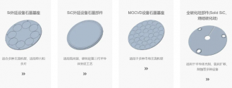
The company's core products are CVD silicon carbide graphite susceptors and thermal field overall solutions for semiconductor epitaxial equipment, which are core components in the field of semiconductor epitaxial equipment. Products include: graphite susceptors for silicon carbide epitaxial equipment, graphite components for silicon carbide epitaxial equipment, graphite susceptors for MOCVD equipment, all-silicon carbide components (Solid SiC, sintered silicon carbide), pure graphite products, etc. The products are mass-produced and supplied to many benchmark customers in the fields of Si semiconductors, SiC, GaN and other third-generation semiconductors and LED optoelectronics.

Please, Log in or Register to view URLs content!
 

tokenanalyst

Brigadier
Registered Member

Yaoqi Semiconductor Chip Manufacturing CMP Polishing Liquid Project Starts Production​


On the morning of September 20, good news came from the Robot Town. The CMP polishing liquid project for semiconductor chip manufacturing of Ningbo Pingheng Electronic Materials Co., Ltd., a holding company of Ningbo Runping Electronic Materials Co., Ltd., was officially put into production. It is reported that the project mainly produces four categories of products: cerium oxide polishing liquid, metal tungsten polishing liquid, oxide polishing liquid, and polysilicon polishing liquid. Among them, the polysilicon polishing liquid has achieved 100% localization of the entire chain from polishing particles to final products, which is of great significance to ensuring the security and stability of China's semiconductor materials industry chain.​

Please, Log in or Register to view URLs content!
 

tinrobert

Junior Member
Registered Member
keep in mind that @tinrobert relies on subscription to earn a living. The link he was providing was the deep dive, which requires a subscription.

What you posted is fine, since it's directly from his substack, but please don't take content from his paid section and put it on pastebin or something like that.
Thank you for mentioning that about my subscription. Here is another article I just posted on Substack. It has a paywall partway through the article, like all my others, but readers can learn about what China is now doing to maintain dominance in rare earths. The linke is:
Please, Log in or Register to view URLs content!

China Tightens Stranglehold on Rare Earths With Strategy To Prevent Western Expansion And Short Circuit Government Effectiveness​


tokenanalyst

Brigadier
Registered Member

Raysolve Unveiled New Production-ready Micro-display Series — PowerMatch®️ 1​


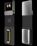
On September 11, the 25th China International Optoelectronic Expo (CIOE 2024) opened in Shenzhen. This event is one of the largest and most influential exhibitions in the optoelectronic industry globally. Raysolve unveiled its new product series, the PowerMatch®️ 1 Full-color Micro-LED Micro-display, which drew significant attention at the expo.The PowerMatch®️ 1 series features a screen size of 0.13 inches and a full-color resolution of 320×240 (Micro-LED resolution of 640×480). The full-color brightness reaches 250,000 nits through process iteration, along with an upgraded CMOS driving architecture, ensuring both high performance and low power consumption.
1727123740629.png
Raysolve’s proprietary quantum dots (QDs) lithography technology combines the high efficiency of QDs with the high resolution of lithography, enabling fine pixel definition through standard semiconductor processes. It allows for high-yield production of full-color Micro-LED micro-displays. The display achieves an impressive color performance of 108.5% DCI-P3 wide color gamut and high color purity.​

Please, Log in or Register to view URLs content!
 
Top