Chinese semiconductor thread II

tokenanalyst

Brigadier
Registered Member

Huaxin Intelligent, a domestic semiconductor advanced packaging equipment supplier, has completed tens of millions of yuan in A+ round financing this year​


Recently, Huaxin Intelligent, a domestic wafer-level advanced packaging and testing equipment company, announced that it had received tens of millions of yuan in A+ round financing in 2024. Among them: Jinhaitong (stock code 603061), a listed company and a leading integrated circuit test and sorting machine company, invested tens of millions of yuan in industry, and Jiangyin Xiayin Investment invested tens of millions of yuan .

Shenzhen Huaxin Intelligent Equipment Co., Ltd. (hereinafter referred to as Huaxin Intelligent) was established in July 2021. It is a semiconductor wafer-level packaging equipment company integrating professional research and development, production and sales. Huaxin Intelligent 's independently developed wafer-level packaging, testing and sorting equipment has been replaced by domestic products since 2023. It is the first advanced packaging and testing equipment company in China to achieve mass production of wafer-level sorting machines . It has obtained mass production orders from several domestic industry leaders and has reached cooperation with many domestic and foreign leaders . After this round of financing, Huaxin Intelligent will set up a localized wafer-level sorting machine manufacturing base in East China and continue to deepen its presence in the East China market.

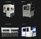
Huaxin Intelligent's main products are advanced packaging, testing, sorting and testing equipment. Advanced packaging, testing, sorting and testing equipment products include WLCSP special sorting equipment, Panel-level packaging, testing and patching equipment, Fanout packaging sorting equipment, SIC KGD equipment, Wafer AOI special equipment, etc.; semiconductor sorting and testing equipment is suitable for advanced packaging such as wafer-level packaging technology (WLCSP), system-level packaging technology (SIP), 2.5/3.0D integrated packaging, Fan-in and Fan-out, Chiplet packaging, etc.
1726933807870.png

Please, Log in or Register to view URLs content!
 

tokenanalyst

Brigadier
Registered Member

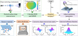
Ultra-precision fabrication technology based on fusion figuring of surface height and slope profile for EUVL objective lenses.​

Abstract​


The manufacturing requirements for extreme ultraviolet lithography (EUVL) projection lenses are highly stringent, demanding ultra-precise control over surface height and slope profile to achieve optimal imaging quality. Nevertheless, the current technology lacks the explicit capability to control the two-dimensional (2D) surface slope of optics. Focusing on the ultra-precision machining technology based on slope profile, a partial derivative exchange decoupling (PDED) method is proposed to approximately calculate the vector removal coupling problem within the 2D slope-based figuring (SF) model, specifically addressing the interplay between the slope removal function and the slope error. Furthermore, the fusion figuring (FF) model accomplishing the dual monitoring of both surface height accuracy and slope profile accuracy is proposed innovatively. Through simulation experiments, the modification results of the fusion, slope-based, and height-based figuring (HF) models are systematically compared and analyzed, demonstrating the effectiveness and superiority of the fusion figuring model. In actual manufacturing experiments, the FF model improves RMS convergence for slope errors by over 20% and for height errors by nearly 10% compared to the HF model. The research results successfully achieve a notable level of convergence in optics machining and provide a new approach with ultra-precision and stability for the fabrication of complex optics requiring precise control of both surface and slope accuracy.

1726941487233.png

Please, Log in or Register to view URLs content!
 

Oldschool

Junior Member
Registered Member
why would i upset ?? you always derail this thread with useless articles.

Digitimes headline -

''China's latest domestically produced DUV exposure machine cannot perform the critical multiple exposures needed for advanced chip production, making it incapable of achieving finer process nodes like 28nm and below''

this is completely wrong, these people continue to make stories on MIIT report, in which China mentioned 65nm dry DUV. and for your kind information 65nm has nothing to do with 28nm and below.. the maximum process that machine can handle is 55nm. so what Digitimes said is completely wrong. these people really don't know anything..

65nm dry DUV has nothing to do with 28nm
We don't know this dry DUV can do 28nm or not. Even thought this machine not meant for 28nm production but No idea how digitimes arrived that

Overlay spec less than equal to 8nm.
Using LELE double patterning, the requirement is 13.5% of half pitch which is 8.775nm .

The spec of less and equal to 8nm meets this. Therefore this dry DUV supports double patterning.

So with double patterning this machine supports resolution of 32.5nm which is entry level for 28nm. We don't know if it actually goes to 28nm but it's very close.

What's digitimes reasoning not supporting multipatterning and goes to 28nm?
 

huemens

Junior Member
Registered Member
We don't know this dry DUV can do 28nm or not. Even thought this machine not meant for 28nm production but No idea how digitimes arrived that

Overlay spec less than equal to 8nm.
Using LELE double patterning, the requirement is 13.5% of half pitch which is 8.775nm .

The spec of less and equal to 8nm meets this. Therefore this dry DUV supports double patterning.

So with double patterning this machine supports resolution of 32.5nm which is entry level for 28nm. We don't know if it actually goes to 28nm but it's very close.

What's digitimes reasoning not supporting multipatterning and goes to 28nm?

This is what they say
Chinese media, citing experts in lithography, noted that a 65nm resolution ArF machine can potentially achieve a 55nm process with optimized optical proximity correction (OPC) algorithms. However, China's DUV machines, with an overlay accuracy of ≤8nm, have too much error to handle multiple exposures, limiting them to 65/55nm processes.
 
  • Like
Reactions: jwt

Oldschool

Junior Member
Registered Member
This is what they say
They are saying it uses OPC and doesn't support double patterning. Well,
overlay accuracy of ≤8nm means it can support double patterning.
It should be able to support 45nm process.
ASML dry DUV supports 45nm

45nm process is commonly used process.

Don't tell me that it has to wait for the ArFi to support 45nm.

Digtimes smells spilling BS.

Anyway, the ArFi definitely an big upgrade with NA 1.35 versus NA 0.9 projection lens ArF.
 

clnt

Just Hatched
Registered Member
They are saying it uses OPC and doesn't support double patterning. Well,
overlay accuracy of ≤8nm means it can support double patterning.
It should be able to support 45nm process.
ASML dry DUV supports 45nm

45nm process is commonly used process.

Don't tell me that it has to wait for the ArFi to support 45nm.

Digtimes smells spilling BS.

Anyway, the ArFi definitely an big upgrade with NA 1.35 versus NA 0.9 projection lens ArF.
45nm is commonly produced with immersion. Only intel used dry double patterning when they developed their process and immersion lithography was very new, but that is not cost efficient nowdays.
 

tphuang

Lieutenant General
Staff member
Super Moderator
VIP Professional
Registered Member

7.5 billion, Tongfu Microelectronics advanced packaging and testing base project started​


On September 20, the official Weibo account of Tongfu Microelectronics announced that the groundbreaking ceremony for the subsidiary Tongfutongda advanced packaging and testing base project was held in Nantong City.

The Tongfu Advanced Packaging and Testing Production Base Project is a major provincial project in 2024, including two sub-projects: Tongfu Tongda and Tongfu Tongke.
The Tongfutongda Advanced Packaging and Testing Base Project, built by Tongfutongda (Nantong) Microelectronics Co., Ltd., was established in March 2023. The total investment of the project is 7.5 billion yuan , of which 3 billion yuan is invested in equipment. After completion, it will mainly involve application fields such as communications, memory, and computing power, focusing on integrated circuit packaging products that are encouraged and supported by the state, such as multi-layer stacking, flip-chip, wafer-level, and panel-level packaging .
The first equipment installation ceremony of the second phase of Tongtian Futongke Memory project was held.

Please, Log in or Register to view URLs content!
advanced packaging project for memory chips.

Is this for HBM? Seems like so.

They are saying it uses OPC and doesn't support double patterning. Well,
overlay accuracy of ≤8nm means it can support double patterning.
It should be able to support 45nm process.
ASML dry DUV supports 45nm

45nm process is commonly used process.

Don't tell me that it has to wait for the ArFi to support 45nm.

Digtimes smells spilling BS.

Anyway, the ArFi definitely an big upgrade with NA 1.35 versus NA 0.9 projection lens ArF.

For economic reasons, I don't think they will ever use this for 45nm process through double patterning.
 

antonius123

Junior Member
Registered Member

[News] Breakthrough in China’s Domestic DUV Equipment to 8nm? Experts Call It a Misunderstanding​


2024-09-18
Please, Log in or Register to view URLs content!
editor

SMEE-624x190.jpg

Recent reports of breakthroughs in China’s chip manufacturing equipment have gained attention, with rumors suggesting that China’s domestically-made DUV equipment can produce chips at 8nm and below. Some companies have also applied for EUV equipment patents. However, according to a report by the
Please, Log in or Register to view URLs content!
, experts believe these claims are questionable, emphasizing that production yield is the real key.

China’s Ministry of Industry and Information Technology recently released a guidance catalog for promoting major technological equipment. Two lithography machines listed have been interpreted by some as a sign of significant technological progress, sparking claims that China can now produce 8nm and more advanced nodes.

Meanwhile, German media outlet
Please, Log in or Register to view URLs content!
reported that Shanghai Micro Electronics applied for a series of EUV-related patents, which may indicate the ability to manufacture chips at 7nm and below.

Huawei’s flagship Mate 60 Pro, launched last year, was reportedly equipped with SMIC’s self-made 7nm chips. Earlier this year, rumors suggested SMIC had successfully produced 5nm chips without EUV machines, which would be used in Huawei’s Mate 70 series set for release later this year. These claims have resurfaced in light of recent developments.

Talks of China breaking through U.S. tech barriers have caught the attention of both domestic and international markets, with many Chinese netizens celebrating on social media. However, while the public cheers, official responses have remained muted. Aside from the ministry’s guidance catalog, no Chinese authorities or companies have confirmed the breakthrough, nor have any real-world applications been showcased.

In reality, since the start of the U.S.-China tech war, China has often hinted at “breaking through technological blockades,” but the results have been largely inconclusive.

Take SMEE, for instance. In June 2020, it announced that it would deliver China’s first domestically-made 28nm immersion lithography machine between 2021 and 2022, model SSA/800-10W. However, the news soon faded. By May 2023, rumors resurfaced that the 28nm machine was nearing completion, and by December, Zhangjiang Group in Shanghai claimed via its official WeChat account that SMEE had successfully developed the 28nm lithography machine. The post was deleted shortly afterward.

As of now, the SSA/800-10W has yet to appear on SMEE’s official product list.

According to a report by Chinese semiconductor media
Please, Log in or Register to view URLs content!
, the lithography machine specifications recently released by the Ministry of Industry and Information Technology show improvements over SMEE’s SSA600 model. However, they still fall short of the capability to produce 28nm chips, let alone 8nm or 7nm chips. The rumors likely stem from a misunderstanding of what the specifications actually mean.

Additionally, a Reuters report from September last year noted that the yield rate for SMIC’s 7nm process was below 50%, whereas the industry standard is 90% or higher. This would significantly constrain chip shipments and impact smartphone production.

Please, Log in or Register to view URLs content!

Can someone clarify?
 

tonyget

Senior Member
Registered Member

[News] Breakthrough in China’s Domestic DUV Equipment to 8nm? Experts Call It a Misunderstanding​


2024-09-18
Please, Log in or Register to view URLs content!
editor

SMEE-624x190.jpg

Recent reports of breakthroughs in China’s chip manufacturing equipment have gained attention, with rumors suggesting that China’s domestically-made DUV equipment can produce chips at 8nm and below. Some companies have also applied for EUV equipment patents. However, according to a report by the
Please, Log in or Register to view URLs content!
, experts believe these claims are questionable, emphasizing that production yield is the real key.

China’s Ministry of Industry and Information Technology recently released a guidance catalog for promoting major technological equipment. Two lithography machines listed have been interpreted by some as a sign of significant technological progress, sparking claims that China can now produce 8nm and more advanced nodes.

Meanwhile, German media outlet
Please, Log in or Register to view URLs content!
reported that Shanghai Micro Electronics applied for a series of EUV-related patents, which may indicate the ability to manufacture chips at 7nm and below.

Huawei’s flagship Mate 60 Pro, launched last year, was reportedly equipped with SMIC’s self-made 7nm chips. Earlier this year, rumors suggested SMIC had successfully produced 5nm chips without EUV machines, which would be used in Huawei’s Mate 70 series set for release later this year. These claims have resurfaced in light of recent developments.

Talks of China breaking through U.S. tech barriers have caught the attention of both domestic and international markets, with many Chinese netizens celebrating on social media. However, while the public cheers, official responses have remained muted. Aside from the ministry’s guidance catalog, no Chinese authorities or companies have confirmed the breakthrough, nor have any real-world applications been showcased.

In reality, since the start of the U.S.-China tech war, China has often hinted at “breaking through technological blockades,” but the results have been largely inconclusive.

Take SMEE, for instance. In June 2020, it announced that it would deliver China’s first domestically-made 28nm immersion lithography machine between 2021 and 2022, model SSA/800-10W. However, the news soon faded. By May 2023, rumors resurfaced that the 28nm machine was nearing completion, and by December, Zhangjiang Group in Shanghai claimed via its official WeChat account that SMEE had successfully developed the 28nm lithography machine. The post was deleted shortly afterward.

As of now, the SSA/800-10W has yet to appear on SMEE’s official product list.

According to a report by Chinese semiconductor media
Please, Log in or Register to view URLs content!
, the lithography machine specifications recently released by the Ministry of Industry and Information Technology show improvements over SMEE’s SSA600 model. However, they still fall short of the capability to produce 28nm chips, let alone 8nm or 7nm chips. The rumors likely stem from a misunderstanding of what the specifications actually mean.

Additionally, a Reuters report from September last year noted that the yield rate for SMIC’s 7nm process was below 50%, whereas the industry standard is 90% or higher. This would significantly constrain chip shipments and impact smartphone production.

Please, Log in or Register to view URLs content!

Can someone clarify?

That's enough. This DUV related news discuss needs to be stopped now
 
Top