Chinese semiconductor thread II

sunnymaxi

Captain
Registered Member
My Googlefeed yesterday had the first few lines of a Techinisghts story that China's (unspecified) DUV machine cannot execute multipatterning and is unable to produce 28nm and smaller nodes. Techinsights website today does not appear to have that story, nor did Google searches reveal it. Did anybody see that story? Did Techinsights withdraw it?
That was not Techinsights. It was a DigiTimes article.
Please, Log in or Register to view URLs content!

I don't have the full text, but most likely it is just a pointless article about the 65nm DUV, as they have been writing various articles about it whole week.
@curiouscat can you please link this article to Pastebin?
we have thoroughly discussed this article before.. if you guys wanting to waste the time please go ahead. page number 458 of this thread..

@curiouscat have already archive this article on your request .. @Wahid145 how could you forget ?? i still don't understand what is your problem ..

see this. i m quoting your old massage here..
@curiouscat could you put this in the Pastebin please? Wanna know what the exparts at Digitimes has to say on this
Please, Log in or Register to view URLs content!
 

huemens

Junior Member
Registered Member
we have thoroughly discussed this article before.. if you guys wanting to waste the time please go ahead. page number 458 of this thread..

@curiouscat have already archive this article on your request .. @Wahid145 how could you forget ?? i still don't understand what is your problem ..

see this. i m quoting your old massage here..

To be fair, it's technically a new article, with a new title. But I agree with you, it's just going to be the same pointless story they have been writing under a different title every 2 days. The one he requested earlier is "Debunking China's first indigenous DUV lithography system" from 16th Sept. Then on 18th they wrote "How far is China from 28nm process after domestic lithography breakthrough?". This one is from 20th "China's homegrown DUV equipment struggles with multiple exposures, hindering chip process advancements". They will probably write a new one tomorrow.
 

Schmoe

New Member
Registered Member
OK. I did not realize its substance had been discussed here previously. It was showing as a "20 hour" old story yesterday but I did not realize it rehashed another article.
 

Wahid145

New Member
Registered Member
we have thoroughly discussed this article before.. if you guys wanting to waste the time please go ahead. page number 458 of this thread..

@curiouscat have already archive this article on your request .. @Wahid145 how could you forget ?? i still don't understand what is your problem ..

see this. i m quoting your old massage here..
You do realize it's a new story right? And it mentions something about multiple exposures too. What's wrong with having a look at it? Surely it doesn't cost an arm and a leg but might contain a few lines of new information at least. Don't get too upset for no reason mate, live your life
 

sunnymaxi

Captain
Registered Member
You do realize it's a new story right? And it mentions something about multiple exposures too. What's wrong with having a look at it? Surely it doesn't cost an arm and a leg but might contain a few lines of new information at least. Don't get too upset for no reason mate, live your life
why would i upset ?? you always derail this thread with useless articles.

Digitimes headline -

''China's latest domestically produced DUV exposure machine cannot perform the critical multiple exposures needed for advanced chip production, making it incapable of achieving finer process nodes like 28nm and below''

this is completely wrong, these people continue to make stories on MIIT report, in which China mentioned 65nm dry DUV. and for your kind information 65nm has nothing to do with 28nm and below.. the maximum process that machine can handle is 55nm. so what Digitimes said is completely wrong. these people really don't know anything..

65nm dry DUV has nothing to do with 28nm
 

tokenanalyst

Brigadier
Registered Member
My Googlefeed yesterday had the first few lines of a Techinisghts story that China's (unspecified) DUV machine cannot execute multipatterning and is unable to produce 28nm and smaller nodes. Techinsights website today does not appear to have that story, nor did Google searches reveal it. Did anybody see that story? Did Techinsights withdraw it?
I course it cannot do 28nm and smaller node, what part of 65nm node is difficult to understand? this is a ArF dry lithography machine with an overlay system to match that process and the same goes for the KrF machine.
When the Immersion lithography machine is publicly announced the final overlay will be probably around 3nm or less and that would be probably capable for 28nm or less.
 

Schmoe

New Member
Registered Member
Note that I did specifically state that I could not tell from the summary if the article was referring to dry DUV or the SAA800.: "that China's (unspecified) DUV machine".
 
Last edited:

tokenanalyst

Brigadier
Registered Member

7.5 billion, Tongfu Microelectronics advanced packaging and testing base project started​


On September 20, the official Weibo account of Tongfu Microelectronics announced that the groundbreaking ceremony for the subsidiary Tongfutongda advanced packaging and testing base project was held in Nantong City.

The Tongfu Advanced Packaging and Testing Production Base Project is a major provincial project in 2024, including two sub-projects: Tongfu Tongda and Tongfu Tongke.
The Tongfutongda Advanced Packaging and Testing Base Project, built by Tongfutongda (Nantong) Microelectronics Co., Ltd., was established in March 2023. The total investment of the project is 7.5 billion yuan , of which 3 billion yuan is invested in equipment. After completion, it will mainly involve application fields such as communications, memory, and computing power, focusing on integrated circuit packaging products that are encouraged and supported by the state, such as multi-layer stacking, flip-chip, wafer-level, and panel-level packaging .
The first equipment installation ceremony of the second phase of Tongtian Futongke Memory project was held.

Please, Log in or Register to view URLs content!
 

tokenanalyst

Brigadier
Registered Member

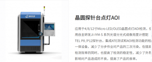
Jingce Electronics' Micro-LED CTAOI testing equipment was successfully delivered to the provincial laboratory​


On September 19, the Micro-LED CT AOI inspection equipment of Jingce Electronics was successfully delivered to a provincial laboratory customer. This laboratory is the first provincial laboratory in the local area approved by the local provincial party committee and government, and is an independent legal entity organized by a local 211 university. This is the first time that the Micro-LED CT AOI equipment independently developed by Jingce Electronics has been successfully delivered in the field of industry-university-research cooperation in university laboratories, marking another important breakthrough for Jingce Electronics in the field of pan-semiconductor inspection.
The wafer appearance inspection equipment independently developed by Precision Electronics is mainly used for front-end and back-end defect detection of semiconductor wafer factories, packaging and testing factories, and Micro-LED and Mini-LED new display wafers: it mainly uses microscopic optical solutions to detect and measure μm-level appearance defects of wafers; it can also be expanded to wafer bumping 3D measurement and LED 3D measurement applications. The software and calculation of the wafer appearance inspection machine are fully independently developed, with independent intellectual property rights, combined with Precision Electronics' many years of technical experience in the field of quality inspection, to promote the localization and application of wafer optical inspection equipment.
The successful delivery of Micro-LED CT AOI inspection equipment in the provincial laboratory is another major breakthrough for Jingce Electronics in the pan-semiconductor inspection board map. In the future, Jingce Electronics will continue to uphold the industry positioning of yield management experts, deepen its brand, cultivate technology, promote the coordinated progress of the pan-semiconductor industry chain, and help the industry develop rapidly.​

1726931390604.png
Please, Log in or Register to view URLs content!
 
Top