You are using an out of date browser. It may not display this or other websites correctly.
You should upgrade or use an alternative browser.
You should upgrade or use an alternative browser.
Chinese semiconductor thread II
- Thread starter vincent
- Start date
Why don't you ask the CEO of AMEC himself?Why do you think there is 14nm<= and 28nm<= if they are exactly the same thing?
View attachment 135579
Tell him he's wrong.
中微公司董事长、总经理尹志尧日前做客《沪市汇·硬科硬客》第十期节目“半导体设备突围关键局”时表示,从设备角度,说老实话,我没有看到(高端领域的)瓶颈。其实有很多人误解说我们做的刻蚀机,有做5纳米刻蚀机、3纳米刻蚀机、14纳米刻蚀机,这个是错误的概念,其实我们同样一个设计,当然有一些改进升级,是一直从45纳米一直做到2纳米都没问题。
yeah. outside Litho all tools are in serial production.. 28nm immersion tools can be used in FinFet process too with little modification/upgradation.. companies don't have choice but to use domestic tools.Seems like they have every tool for 28nm fabrication except for litho. The question is how economically relevant their performance is.
Basic self-sufficiency have achieved in Semi tools..
----------------------------------------------------------------------------------------------------------------------------
AMEC Chairman Yin Zhiyao said that from the equipment point of view, to be honest, I have not seen it (in the high-end field) ) bottleneck. In fact, many people misunderstand that the etching machines we make include 5-nanometer etching machines, 3-nanometer etching machines, and 14-nanometer etching machines. This is a wrong concept. In fact, we have the same design, and of course there are some improvements and upgrades. , it has been no problem from 45 nanometers to 2 nanometers.
Last edited:
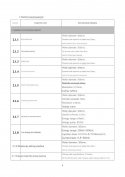
Promote the application of these major technical equipment! The Ministry of Industry and Information Technology issued.
Here are the relevant parts translated:
China's first major technical equipment (set) refers to equipment products that have achieved major technological breakthroughs in China, possess intellectual property rights, and have not yet achieved significant market performance


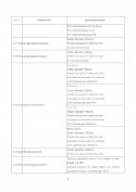
We can see all tools (but litho) can process nodes equal or better than 28nm.
A nice exception CMP that can go to equal of better than 14nm for some materials.
Regarding lithography we have 2 entries:
2.1.5 248nm: KrF litho machine with resolution <= 110nm, note resolution is not process node!
2.1.6 193nm: ArF litho machine with resolution <= 65nm. This is probably the dry version, because the immersion version of DUV has resolution of 38nm.
I can note that overlay specs are quite bad in both cases. For Arf DUV is just <= 8nm. For reference the ASML DUV entry level has overlay of 2.5nm. Overlay is THE critical spec to go down with nodes, you can say it is the most important spec.
We know since almost 2 years there is at least a prototype of DUV immersion machine, so my opinion is that they are quite open on other machines, they clearly state that 28nm node is conquered and very probably also better ones.
Instead for litho, that is the critical piece of equipment, I see there is still a lot of fog: no mention to immersion DUVi + unrealistically bad overlay specs.
Are the projects listed there completed or planned?Promote the application of these major technical equipment! The Ministry of Industry and Information Technology issued.
Note the DUV
View attachment 135571
You should not be comparing a dry ArF tool with an immersion one. But it is still pretty bad.I can note that overlay specs are quite bad in both cases. For Arf DUV is just <= 8nm. For reference the ASML DUV entry level NXT:1980Fi has overlay of 2.5nm. Overlay is THE critical spec to go down with nodes, you can say it is the most important spec.
KrF tool by ASML with <= 5nm overlay:
Dry ArF tool by ASML with <= 4.5 nm overlay:
KrF tool by Canon with <= 5nm overlay:
KrF tool by Nikon with <= 6 nm overlay:
Dry ArF tool by Nikon with <= 5 nm overlay:
I have read each and every page of this thread since probably like a year. But even I am totally confused. I can swear, I had the impression from previous posts that 28 nm lithography was already solved. Is there a better thread to discuss what can be done to streamline information in this thread? For e.g. Maybe there can be a "micro"-semiconductor thread where you debate and post minutae like patent filings, but a "macro"-semiconductor thread which talks about bigger "macro" trends.
28nm immersion machine SSA800i currently pattering wafers in fab .. if you remember, Suppliers of SMEE like RSLaser and others have started mass production this year.. this is an another indication.I have read each and every page of this thread since probably like a year. But even I am totally confused. I can swear, I had the impression from previous posts that 28 nm lithography was already solved. Is there a better thread to discuss what can be done to streamline information in this thread? For e.g. Maybe there can be a "micro"-semiconductor thread where you debate and post minutae like patent filings, but a "macro"-semiconductor thread which talks about bigger "macro" trends.
DUV/DUVi problems not only solved but all technical glitches fixed too.. this was even confirmed by havoc itself.
Here are the relevant parts translated:
View attachment 135581
View attachment 135582
We can see all tools (but litho) can process nodes equal or better than 28nm.
A nice exception CMP that can go to equal of better than 14nm for some materials.
Regarding lithography we have 2 entries:
2.1.5 248nm: KrF litho machine with resolution <= 110nm, note resolution is not process node!
2.1.6 193nm: ArF litho machine with resolution <= 65nm. This is probably the dry version, because the immersion version of DUV has resolution of 38nm.
I can note that overlay specs are quite bad in both cases. For Arf DUV is just <= 8nm. For reference the ASML DUV entry level has overlay of 2.5nm. Overlay is THE critical spec to go down with nodes, you can say it is the most important spec.
We know since almost 2 years there is at least a prototype of DUV immersion machine, so my opinion is that they are quite open on other machines, they clearly state that 28nm node is conquered and very probably also better ones.
Instead for litho, that is the critical piece of equipment, I see there is still a lot of fog: no mention to immersion DUVi + unrealistically bad overlay specs.
Havok already talked about CETC 65nm dry Arf machine two years ago. I believe the machine on the list is this CETC machine they are referring to
it's important to not over rely on one document. IIRC, the general specs for SMEE machines were targeting comparable ASML models. Also, the big issue with SMEE machines were their software and reliability. All things that can only improve over time and through a lot of trial production. That's what I assume is going on right now.
I assume at this point that at least some lines are using dry Arf scanner from SMEE. It's unclear where the immersive Arf scanner is at. But I also don't think that's particularly important.
I assume at this point that at least some lines are using dry Arf scanner from SMEE. It's unclear where the immersive Arf scanner is at. But I also don't think that's particularly important.
