You are using an out of date browser. It may not display this or other websites correctly.
You should upgrade or use an alternative browser.
You should upgrade or use an alternative browser.
Chinese semiconductor thread II
- Thread starter vincent
- Start date
Honghui Integration received investment from Guofa Venture Capital, focusing on the clean room system integration solution track
According to the news from Guofa Ventures, Suzhou Suchuang Manufacturing Investment Partnership (Limited Partnership), a subsidiary of Suzhou Suchuang Investment and Guofa Ventures, has recently officially invested in Honghui System Integration Technology (Jiangsu) Co., Ltd. (hereinafter referred to as Honghui Integration). This round of financing is exclusively invested by Suzhou Suchuang Investment and Guofa Ventures, totaling 20 million yuan. This round of funds will be mainly used for technology research and development and market development.
Honghui System Integration Technology (Jiangsu) Co., Ltd. was established in November 2011 and is located in Kunshan City, Suzhou City, Jiangsu Province. It mainly focuses on providing professional clean room system integration solutions for high-tech industries' factory construction, technical transformation and other projects, covering new energy, electronic semiconductors, supercomputing centers, biomedicine, food and beverage and other industries. It is one of the few clean room system integration solution providers in China that can undertake mainstream projects in multiple industries.
It is reported that the company's main customers involve multiple industries, including the new energy industry including CATL, Envision New Energy, GCL Solar, etc.; the electronic semiconductor industry including AMD, Visionox, etc.; the supercomputing center includes Alibaba, etc.
Zhejiang University New Immersion Lithography Coating Material Technology
Immersion boundary flow field convergence and removal method for IC lithography equipment based on organic medium.
CN118483879A
Abstract
The present invention discloses a method for converging and removing the immersion boundary flow field of an IC lithography device based on an organic medium. A super oleophobic coating is uniformly sprayed on the part of the substrate of the IC lithography device where the immersion liquid is not fully recovered, and then a heat treatment is performed; the immersion boundary flow field is filled with the immersion liquid through an immersion supply system to complete the converging; at the same time, the immersion liquid flows out for recovery; the immersion liquid is recovered through the immersion supply system until it completely flows out, and the removal is completed. The present invention sprays a super oleophobic coating on the part where the immersion liquid is not fully recovered, which can increase the contact angle of the fluid on the surface of the substrate without affecting the exposure conditions and the fluid properties, improve the flow characteristics of the fluid on the substrate, eliminate fluid residues, and achieve the effects of uniform and complete filling and complete recovery of the organic medium; the present invention does not need to change the structure of the substrate itself, improves the use efficiency of the organic medium, reduces costs while improving production efficiency, and ultimately improves the exposure quality.
Tbps wide-field parallel optical wireless communications based on a metasurface beam splitter
Abstract
Optical wireless communication (OWC) stands out as one of the most promising technologies in the sixth-generation (6G) mobile networks. The establishment of high-quality optical links between transmitters and receivers plays a crucial role in OWC performances. Here, by a compact beam splitter composed of a metasurface and a fiber array, we proposed a wide-angle (~120°) OWC optical link scheme that can parallelly support up to 144 communication users. Utilizing high-speed optical module sources and wavelength division multiplexing technique, we demonstrated each user can achieve a communication speed of 200 Gbps which enables the entire system to support ultra-high communication capacity exceeding 28 Tbps. Furthermore, utilizing the metasurface polarization multiplexing, we implemented a full range wide-angle OWC without blind area nor crosstalk among users. Our OWC scheme simultaneously possesses the advantages of high-speed, wide communication area and multi-user parallel communications, paving the way for revolutionary high-performance OWC in the future.The first phase of the National Big Fund invested in the domestic EDA manufacturer Hongxin Micronano: invested nearly 500 million yuan and held 38.7% of the shares.
on September 4, domestic EDA manufacturer Shenzhen Hongxin Micronano Technology Co., Ltd. (hereinafter referred to as "Hongxin Micronano") underwent industrial and commercial changes, adding Shenzhen Guidance Fund Investment Co., Ltd., National Integrated Circuit Industry Investment Fund Co., Ltd. (National Integrated Circuit Industry Investment Fund Phase I), and Hongxin Venture Capital (Shenzhen) Enterprise (Limited Partnership) as shareholders.
ccording to information, Hongxin Micronano was established in 2018 and is a high-tech company dedicated to the research, development, production and sales of domestic digital chip electronic design automation (EDA). It aims to complete the technical deployment of key nodes of digital EDA through independent research and development, technology introduction, cooperative development and other modes, build a complete domestic digital chip full-process tool chain, and achieve technological breakthroughs in the industrial chain; the company relies on the complete domestic industrial ecology, establishes a professional R&D and support team, builds a competitive technology platform, and is committed to providing a full range of solutions and technical services for the global chip design industry in a wide range of application fields.
The company's R&D centers in Shenzhen, Shanghai, Beijing and Chengdu have gathered outstanding talents from home and abroad, all of whom come from internationally renowned EDA and design companies, with an average of 10 years of R&D experience. By independently completing the tape-out of complex projects, it has won the recognition of commercial customers including domestic advanced design companies.
Sanze New Materials: The second phase of the high-precision structural ceramics industrialization project for semiconductor equipment has been capped.
On September 2, Jiangsu Sanze New Materials Technology Co., Ltd. held a topping-out ceremony for the second phase of the high-precision structural ceramics industrialization project for semiconductor equipment in Nantong. Structural ceramics are mainly based on the mechanics and structural uses of materials, and have the characteristics of high strength, high hardness, high temperature resistance, corrosion resistance, and oxidation resistance.
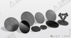
In terms of market share, functional ceramics account for 79%, while structural ceramics account for 21%. With the continuous advancement of technology, structural ceramics have become an indispensable material for promoting the precision and high efficiency of the semiconductor industry, especially in the manufacturing of semiconductor equipment, where structural ceramics play a key role. SiC ceramic materials often show excellent high-temperature strength, corrosion resistance, high hardness and thermal conductivity, becoming one of the most widely used structural ceramic materials. In the semiconductor field, silicon carbide material parts have the characteristics of low density, high thermal conductivity, high bending strength, and large elastic modulus. They can adapt to the strong corrosive and ultra-high temperature harsh reaction environment of wafer epitaxy and etching manufacturing links. Therefore, they are widely used in major semiconductor equipment such as epitaxial growth equipment, etching equipment, oxidation/diffusion/annealing equipment.

In terms of market share, functional ceramics account for 79%, while structural ceramics account for 21%. With the continuous advancement of technology, structural ceramics have become an indispensable material for promoting the precision and high efficiency of the semiconductor industry, especially in the manufacturing of semiconductor equipment, where structural ceramics play a key role. SiC ceramic materials often show excellent high-temperature strength, corrosion resistance, high hardness and thermal conductivity, becoming one of the most widely used structural ceramic materials. In the semiconductor field, silicon carbide material parts have the characteristics of low density, high thermal conductivity, high bending strength, and large elastic modulus. They can adapt to the strong corrosive and ultra-high temperature harsh reaction environment of wafer epitaxy and etching manufacturing links. Therefore, they are widely used in major semiconductor equipment such as epitaxial growth equipment, etching equipment, oxidation/diffusion/annealing equipment.
metal oxide hardmask resist is critical for EUV. Sn has a high EUV photon absorption cross section but V is very low. Wonder what the function of V is - maybe some sort of energy transfer mechanism to the alkyl chains? Patents won't go deep into this I think. Need an original paper.

