You are using an out of date browser. It may not display this or other websites correctly.
You should upgrade or use an alternative browser.
You should upgrade or use an alternative browser.
Chinese semiconductor thread II
- Thread starter vincent
- Start date
I posted a machine translation of that ZDNet Korea article in Chinese semiconductor thread II.
From other posts I have seen CXMT is likely producing 5% of world DRAM as of late last year and this production will rise to 10% when they finish their second fab module. Doubling production from 100,000 wpm to 200,000 wpm. In their business plan a third expansion to 300,000 wpm total is also planned in the future.
You can see a decent resolution (albeit old) satellite picture of the CXMT fabs at Hefei in Chinese semiconductor thread II.
Here is a recent low resolution Sentinel-2 satellite photo from August 26th.

On the right you can see FAB 1 on top and FAB 2A and 2B below that.
The original plan was for CXMT FAB 2 to be an exact copy of FAB 1. Instead they split it into two buildings. The same thing happened with YMTC FAB 2. I have my guesses as to why, I suspect this was done so they can run two different process lines. Perhaps one with US tools in it, and another without.
The bigger question is what about Fujian Jinhua and that other DRAM manufacturer that Unigroup was supposedly setting up. Fujian Jinhua won the lawsuit against Micron in the US. So their sanctions on purchasing and maintaining chip equipment should be lifted no? At least one would hope so.
From other posts I have seen CXMT is likely producing 5% of world DRAM as of late last year and this production will rise to 10% when they finish their second fab module. Doubling production from 100,000 wpm to 200,000 wpm. In their business plan a third expansion to 300,000 wpm total is also planned in the future.
You can see a decent resolution (albeit old) satellite picture of the CXMT fabs at Hefei in Chinese semiconductor thread II.
Here is a recent low resolution Sentinel-2 satellite photo from August 26th.

On the right you can see FAB 1 on top and FAB 2A and 2B below that.
The original plan was for CXMT FAB 2 to be an exact copy of FAB 1. Instead they split it into two buildings. The same thing happened with YMTC FAB 2. I have my guesses as to why, I suspect this was done so they can run two different process lines. Perhaps one with US tools in it, and another without.
The bigger question is what about Fujian Jinhua and that other DRAM manufacturer that Unigroup was supposedly setting up. Fujian Jinhua won the lawsuit against Micron in the US. So their sanctions on purchasing and maintaining chip equipment should be lifted no? At least one would hope so.
Last edited:
North Huachuang: The company's self-developed RF power supply has been applied in batches to many products
North Huachuang stated on an interactive platform that with the rapid improvement in the capabilities of domestic component suppliers in recent years, the company's domestic procurement ratio has also increased year by year, and the company's self-developed RF power supply has been applied in batches to a number of products.
It is reported that NAURA's product line is constantly innovating and improving, and the platform layout is accelerating development. The company has successfully developed a number of high-end equipment with independent intellectual property rights, such as high-density plasma chemical vapor deposition (HDPCVD), dual Damascus CCP etcher, vertical furnace atomic layer deposition (ALD), high dielectric constant atomic layer deposition (ALD), etc., and has achieved stable mass production in many clients.
At the same time, the company has made a comprehensive layout in the field of advanced packaging and can provide comprehensive solutions for TSV (through silicon via) manufacturing, front process-Damask process, back process-copper etching and RDL (rewiring layer) process, involving more than 20 equipment and process solutions in four major categories: etching, thin film, furnace tubes, and cleaning.
AMEC signed MOCVD project in Nanchang, focusing on GaAs-based red and yellow LED applications
On September 6, the MOCVD equipment development project for GaAs-based red-yellow LED applications of Nanchang AMEC was signed in Nanchang. Gao Shiwen, Deputy Secretary of the Nanchang Municipal Party Committee and Acting Mayor, Song Dexiong, Director of the Jiangxi Provincial Department of Science and Technology, and Yin Zhiyao, Chairman and General Manager of AMEC (Shanghai) Co., Ltd., delivered speeches and witnessed the signing together.
Gao Shiwen said in his speech that the Zhongwei MOCVD equipment development project, as the first special major project in the province, landed in Nanchang. It is not only the fruit of the close cooperation between the two sides in the early stage, but also the "new bud" of the two sides continuing to work together based on a common vision. Nanchang will vigorously implement the "8810" action plan, continue to exert its strength in the electronic information industry, continuously enhance its technological advantages, enhance its industrial advantages, and expand its market advantages, so as to provide a broader space and stage for the development of Zhongwei. After the successful development of the Zhongwei project, it will break through the key technologies of MOCVD equipment and fill the gaps in this field in China. It is believed that it will definitely inject new strong momentum into the development of Nanchang's advanced manufacturing industry and new quality productivity. Nanchang City will do its best to be a good "host" and a good "shop assistant", and fully support Zhongwei Company and Zhongwei's suppliers and customers to invest, start businesses, and grow in Chang. It is hoped that Nanchang High-tech Zone will continue to be the "strongest backing" for the development of Zhongwei Company, take the initiative, provide front-line services, and do everything possible to promote the early implementation and early results of the project. We hope that AMEC will further take root in Nanchang and develop its presence in Nanchang, bring more research and development layouts, leading technologies, and innovative businesses to Nanchang, and share opportunities and develop together with Nanchang.
Kaishitong Semiconductor signed a strategic cooperation agreement with domestic upstream and downstream integrated circuit companies
On September 9, a seminar and signing ceremony was held in Pudong, Shanghai, with the theme of localization of components and new quality productivity. Kaishitong Semiconductor, a subsidiary of Wanye Enterprise, and several other units participated in the event. At the meeting, all parties signed a strategic cooperation agreement to promote the integrated development of component companies to meet the challenges of local chip manufacturing.
Kaishitong Semiconductor, a subsidiary of Wanye Enterprise, has signed cooperation agreements with domestic integrated circuit manufacturers, the Institute of Plasma Physics of the Hefei Institutes of Physical Science, Chinese Academy of Sciences, and other units. The cooperation covers the research and development and supply of key components such as microwave plasma spray guns, electrostatic chuck materials, vacuum automation robots, ultra-high energy radio frequency accelerators, radio frequency power supplies, and high-precision gas flow meters.
Jiufengshan Laboratory has attracted nearly 30 semiconductor companies to gather, with a total valuation of over 10 billion!
In March 2023, the Hubei Jiufengshan Laboratory, which focuses on compound semiconductor research and development and innovation, was officially put into operation.
After one year of operation, the Jiufengshan Laboratory has achieved the operation of the 8-inch pilot line, and the first batch of wafers (high-precision gratings) have been successfully rolled off the production line, filling the gap in the domestic production process of high-line density, ultra-high refractive index, and non-periodic high-precision gratings.
The world's first 8-inch silicon photonic thin-film lithium niobate optoelectronic integrated wafer was also successfully rolled off the production line in March this year. It can realize large-scale manufacturing of high-end optical chips with ultra-low loss and ultra-high bandwidth, and is currently the world's best optoelectronic integrated chip with the best overall performance.
In addition to its own continuous innovation and breakthroughs, as one of the few public, open, neutral and shared scientific research platforms in China, Jiufengshan Laboratory also works closely with leading companies in the industrial chain, takes "use" as the guide, plans to develop common technologies, promotes the verification of domestic semiconductor materials and equipment, and builds a compound semiconductor pilot platform.
In the Jiufengshan Laboratory, hundreds of projects are running simultaneously in the 9,000-square-meter clean room, and scientific researchers and industrial chain companies are engaged in joint research and development everywhere in the laboratory.
The etching and thin film deposition equipment developed by Shanghai Bangxin Semiconductor Technology Co., Ltd. has achieved mass production of multiple devices with the help of Jiufengshan Laboratory.
Wuhan Yitiannuo Technology Co., Ltd. and Jiufengshan Laboratory have jointly developed silicon photonics and third-generation semiconductor wafer-level, chip-level, and device-level packaging and testing equipment with testing accuracy reaching the micron level.
The first set of high-end semiconductor wafer laser cutting equipment developed by HGTECH passed the pilot verification with the help of Jiufengshan laboratory platform, and the equipment that obtained the test report has been successfully introduced to downstream enterprises.

High-Efficiency Reflective Focusing in Extreme Ultraviolet with Multilayer Metalens
Tongji UniversityAbstract
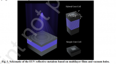
The focusing of extreme ultraviolet light is essential for high-precision lithography, high-resolution imaging, and fine measurement. The investigation of extreme ultraviolet metalens presents significant opportunities for advancing metaoptics. However, the transmissive extreme ultraviolet metalens suffers from low efficiency due to high-order diffraction. Here, we propose a high-efficiency extreme ultraviolet reflective metalens composed of multilayer films and vacuum holes. By means of meticulous design and structural optimization, the reflective configurations based on multilayer films support a complete 2π phase profile in a small period with high-efficiency meta-atoms. The extreme ultraviolet reflective metalens with a numerical aperture of 0.05 achieves a high-quality focusing profile with a relative focusing efficiency of 65.77% and an absolute focusing efficiency of 15.80%. Comparisons with other works highlight the superiority of our design. The absolute focusing efficiency of the proposed extreme ultraviolet reflective metalens is twice that of previously reported works, demonstrating that high-order diffraction can be effectively suppressed not only by reducing the period but also by incorporating multilayer films. This work demonstrates a high-efficiency extreme ultraviolet reflective metalens and elucidates its underlying physical mechanism, paving the way for advanced extreme ultraviolet light manipulation.


Direct Monitoring of Nanoscale Deformations across All Layers in Three-Dimensional Stacked Structures.
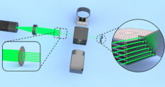
Due to its high bandwidth, low latency, low power consumption, and compact size, three-dimensional (3D) integration of semiconductor chips holds the promise of boosting the performance of integrated circuit systems. However, the applications of 3D stacked structures are constrained by the surface deformation of each thin layer induced by thermal effects, vibration, gravity, and other environmental stresses. Therefore, ensuring the performance and reliability of 3D stacked structures necessitates the precise measurement of nanoscale deformation in each layer. Furthermore, the spacing between layers in 3D stacked structures using modern microelectronics and packaging technologies is exceedingly small, making it impossible to measure the deformation of all layers. Here, we present a novel optical endoscope that fuses a miniaturized interferometry array, a laser-fabricated microprobe, and a highly efficient profile reconstruction algorithm for the precise measurements of surface deformation across all layers in 3D stacked structures. Our method offers a potentially effective and noninvasive way to address the challenges associated with in-line deformation measurement across all layers in real 3D stacked wafers and chips.

Gray market imports. Russia is doing the same thing.
They cannot easily stop such imports when these products are so commonly available.
The only way to stop it would be to require strict export licenses on a per customer basis like they used to do with Cray computers back in the Cold War. But this would make those chips a boutique product and possibly uneconomical to develop.
Renting chips is not worth it. All resources should focused on developing and buying local chips.

