Interesting patent from AMEC for an integrated etching-deposition tool for making ultra high aspect ratio holes.


Wafer processing method and integrated etch deposition device for wafer processing
WO2024125303A1
Abstract
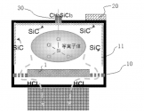
The present invention discloses a wafer processing method and an integrated etching deposition device for wafer processing. The method comprises: providing a plasma processing apparatus; providing a wafer to be processed and placing said wafer in a plasma processing chamber; starting a plasma radio frequency source and introducing an etching gas to etch an etching area, so as to form a hole or a trench; and performing monitoring and, according to a monitoring condition, performing a change to introduce a first mask precursor to deposit a mask or introduce the etching gas to continue etching until it is detected that the hole or trench formed in the etching area meets a target etching requirement, wherein the first mask precursor contains methylsilane as a substitute. In the present invention, by means of real-time monitoring, the operation mode of wafer processing can be changed to an etching mode or a mask deposition mode, so that in situ etching or in situ mask deposition is performed on a wafer to be processed, and it is unnecessary to remove said wafer from a plasma processing chamber, thereby reducing costs and shortening the production period. The present invention is applicable to the etching of a large-size silicon hole, and is also applicable to the etching of a microstructure of a high or ultra-high aspect ratio.
