Horizon Robotics announces 6 million delivery of its journey series of ADAS chips.
You are using an out of date browser. It may not display this or other websites correctly.
You should upgrade or use an alternative browser.
You should upgrade or use an alternative browser.
Chinese semiconductor thread II
- Thread starter vincent
- Start date
China's chips have collectively exploded, with profits of 57 companies increasing by 200%, setting a new record?
It has to be said that the more the United States suppresses China's chip industry, the faster China's chip industry is rising, and its technology, processes and production capacity are growing beyond U.S. expectations.
Recently, some media counted the performance of listed semiconductor companies in the first half of the year and found that 57 companies have announced their performance. The combined net profit of these 57 companies increased by 200% year-on-year to about 13.5 billion yuan. This is another new record second only to 2022.
Why are these listed companies performing so well? The reason is simple: the global semiconductor industry is currently recovering, and China, as the world's largest chip demand market, is naturally recovering faster.
Chinese semiconductor companies can be said to be in a good position to take advantage of the market. On the one hand, they are stimulated by market demand, and on the other hand, they naturally benefit from domestic substitution.
At present, many domestic companies, when using chips, if there is no substitute, they will naturally adopt imported chips, but if they can be replaced by domestic products, they will of course replace them with domestic products. Therefore, the revenue of domestic semiconductor companies has increased significantly, and the profit has increased by 200%.

According to data from US media, mainland China currently ranks first in the world in chip production capacity, with a production capacity ratio of up to 24%, surpassing all countries and regions in the world including Taiwan, South Korea, and Japan.
In addition, the US media predicts that in the next 10 years, mainland China's chip production capacity will continue to remain first. By 2032, the proportion may drop to around 21%, but it will still be first in the world.
Data shows that there are currently 44 wafer fabs in mainland China, and 22 wafer fabs are under construction, which are expected to be completed within three years. Once completed, the production capacity of mature chips may increase by 30-50%.
In addition, more than 10 wafer fabs are planned for the long term and may be started in the next 3-5 years.
Because China's chip production expansion is so rapid, American experts have previously stated that although China is developing mature chips on a large scale, its operating costs are the lowest in the world due to its cheap labor, sound industrial system, and the time is right. I'm afraid that China's mature chips will take over the world.

Once mature chips are occupied by Chinese companies, it will promote the development and inclination of the entire supply chain. Eventually, China will definitely make breakthroughs in advanced chips and eventually sweep the world.
Of course, this is somewhat exaggerated, but it is undeniable that if China continues to expand production, even if it currently focuses on mature chips, it will definitely make breakthroughs in advanced chips in the future and become the global chip overlord. This is only a matter of time.
It has to be said that the more the United States suppresses China's chip industry, the faster China's chip industry is rising, and its technology, processes and production capacity are growing beyond U.S. expectations.
Recently, some media counted the performance of listed semiconductor companies in the first half of the year and found that 57 companies have announced their performance. The combined net profit of these 57 companies increased by 200% year-on-year to about 13.5 billion yuan. This is another new record second only to 2022.

Why are these listed companies performing so well? The reason is simple: the global semiconductor industry is currently recovering, and China, as the world's largest chip demand market, is naturally recovering faster.
Chinese semiconductor companies can be said to be in a good position to take advantage of the market. On the one hand, they are stimulated by market demand, and on the other hand, they naturally benefit from domestic substitution.
At present, many domestic companies, when using chips, if there is no substitute, they will naturally adopt imported chips, but if they can be replaced by domestic products, they will of course replace them with domestic products. Therefore, the revenue of domestic semiconductor companies has increased significantly, and the profit has increased by 200%.

According to data from US media, mainland China currently ranks first in the world in chip production capacity, with a production capacity ratio of up to 24%, surpassing all countries and regions in the world including Taiwan, South Korea, and Japan.
In addition, the US media predicts that in the next 10 years, mainland China's chip production capacity will continue to remain first. By 2032, the proportion may drop to around 21%, but it will still be first in the world.
Data shows that there are currently 44 wafer fabs in mainland China, and 22 wafer fabs are under construction, which are expected to be completed within three years. Once completed, the production capacity of mature chips may increase by 30-50%.
In addition, more than 10 wafer fabs are planned for the long term and may be started in the next 3-5 years.
Because China's chip production expansion is so rapid, American experts have previously stated that although China is developing mature chips on a large scale, its operating costs are the lowest in the world due to its cheap labor, sound industrial system, and the time is right. I'm afraid that China's mature chips will take over the world.

Once mature chips are occupied by Chinese companies, it will promote the development and inclination of the entire supply chain. Eventually, China will definitely make breakthroughs in advanced chips and eventually sweep the world.
Of course, this is somewhat exaggerated, but it is undeniable that if China continues to expand production, even if it currently focuses on mature chips, it will definitely make breakthroughs in advanced chips in the future and become the global chip overlord. This is only a matter of time.
China Resources Shanghua's patent for "Semiconductor device with isolation structure and manufacturing method thereof" was published
According to Tianyancha, the patent of "Semiconductor device with isolation structure and manufacturing method thereof" of Wuxi China Resources Shanghua Technology Co., Ltd. was announced. The application publication date is August 9, 2024, and the application publication number is CN118472028A.
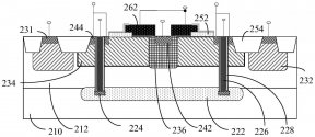
The present invention relates to a semiconductor device with an isolation structure, comprising: a substrate having a second conductivity type; a first conductive buried layer having a first conductivity type and located in the substrate; the first conductivity type and the second conductivity type are opposite conductivity types; a first pole doping region having the first conductivity type and located above the first conductive buried layer; a second pole doping region having the first conductivity type and located above the first conductive buried layer and on both sides of the first pole doping region; an isolation structure, comprising an insulating layer located on the sidewall of an isolation groove, the isolation groove extending downward from the second pole doping region to the first conductive buried layer, and a conductive structure electrically connected to the first conductive buried layer is also provided in the isolation groove. The present invention sets an isolation groove extending downward to the first conductive buried layer at the position of the second pole doping region, reuses the chip area of the second pole doping region, and thus the chip area utilization rate is high.
According to Tianyancha, the patent of "Semiconductor device with isolation structure and manufacturing method thereof" of Wuxi China Resources Shanghua Technology Co., Ltd. was announced. The application publication date is August 9, 2024, and the application publication number is CN118472028A.

The present invention relates to a semiconductor device with an isolation structure, comprising: a substrate having a second conductivity type; a first conductive buried layer having a first conductivity type and located in the substrate; the first conductivity type and the second conductivity type are opposite conductivity types; a first pole doping region having the first conductivity type and located above the first conductive buried layer; a second pole doping region having the first conductivity type and located above the first conductive buried layer and on both sides of the first pole doping region; an isolation structure, comprising an insulating layer located on the sidewall of an isolation groove, the isolation groove extending downward from the second pole doping region to the first conductive buried layer, and a conductive structure electrically connected to the first conductive buried layer is also provided in the isolation groove. The present invention sets an isolation groove extending downward to the first conductive buried layer at the position of the second pole doping region, reuses the chip area of the second pole doping region, and thus the chip area utilization rate is high.
The Institute of Microelectronics of the Chinese Academy of Sciences has made new progress in organic in-sense computing
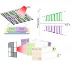
With the rapid development of artificial intelligence technology, the surge in sensor data has posed severe challenges to data processing speed and energy efficiency. Traditional sensor architectures (such as the von Neumann architecture) physically separate sensing, computing, and storage units, and their large amounts of data conversion and transmission further increase energy consumption and time delays. To meet this challenge, researchers have proposed an advanced sensor architecture, in-sense computing technology, which can simultaneously perceive and process images at the sensor level. Organic semiconductors have attracted much attention due to their intrinsic flexibility and adjustable band gap, especially in near-infrared (NIR) optoelectronic applications, which have great potential applications such as fluorescence imaging, medical monitoring, remote sensing, and optical communications. However, organic optoelectronic devices still face huge challenges in realizing intelligent sensing, especially in-sense computing.
Recently, the team of Academician Liu Ming/Researcher Li Mengmeng from the Institute of Microelectronics has developed a new heterojunction structure composed of partially overlapping p-type and n-type organic semiconductor materials. The structure can be processed using conventional photolithography technology and can achieve an integration density of up to 520 devices per square centimeter and a channel length of 5 microns. The heterojunction uses the light gating effect to achieve positive and negative responses to near-infrared light (>1000 nm). More importantly, the photoresponsivity of the heterojunction is linearly related to the gate voltage, and real-time matrix multiplication operations can be performed in the sensor, realizing efficient and accurate near-infrared sensor computing functions including image processing and non-destructive reading and classification, providing new routes and new ideas for the development and application of organic electronics in the next generation of intelligent sensory systems.
This work was supported by the National Key R&D Program and the National Natural Science Foundation of China. The research results were published in the recent Advanced Materials under the title "Gate-Tunable Positive and Negative Photoconductance in Near-Infrared Organic Heterostructures for in-Sensor Computing", and were selected as Editors' Choice highlights and as the inside back cover of the journal. Xu Yunqi, a graduate student at the Institute of Microelectronics, is the first author of the paper, and Li Mengmeng, a researcher at the Institute of Microelectronics, is the corresponding author.

Last edited:
The BIT team has made important progress in portable flexible X-ray detection system
Recently, the Institute of Flexible Electronic Devices and Intelligent Manufacturing, School of Integrated Circuits and Electronics, Beijing Institute of Technology, published an academic paper titled "Flexible single microwire X-ray detector with ultrahigh sensitivity for portable radiation detection system" in Advanced Materials. The paper reports a portable flexible X-ray detection system for radiation detection, which achieves effective monitoring of low-dose X-rays under ambient light, reduces the dependence of conventional X-ray detectors on packaging materials, and promotes the development of X-ray detection systems towards flexibility and miniaturization. Beijing Institute of Technology is the first unit, and the cooperating units include Zhengzhou University. Chen Yan, a postdoctoral fellow at Beijing Institute of Technology, became the first author of the paper, and Associate Professor Li Ying, Professor Shen Guozhen and Professor Shan Chongxin of Zhengzhou University are the corresponding authors.
Flexible X-ray detectors that directly convert X-rays into electrical signals have great application potential in medicine, industry, security, and scientific research. However, current semiconductor-based direct X-ray detectors often have disadvantages such as large size, fragility, and susceptibility to interference from ambient light, which hinders their application in the field of flexible wearable electronic devices.
This paper reports a flexible solar-blind X-ray detector based on a single micrometer wire of indium-doped gallium oxide (Ga2O3:In). Thanks to the high crystal quality, wide bandgap characteristics and high X-ray absorption coefficient of Ga2O3:In micrometer wire, the prepared Ag/Ga2O3:In/Ag detector has an ultra-high sensitivity of 5.9×10⁵μC Gyair-1 cm-2, a detection limit of 67.4 nGyair s-1 and a low false alarm rate. In addition, the flexible device can still work normally at a high temperature of 200 ℃, with excellent working stability and high temperature stability. Finally, the device is integrated into a portable X-ray detection system, which can monitor X-rays in ambient light in real time, prevent the harm caused by X-ray leakage, and display the monitoring results on the user's mobile phone interface.
Through material synthesis, experimental research and theoretical verification, the paper prepared a flexible X-ray detector with high sensitivity and low false alarm rate, realizing real-time monitoring and early warning of X-rays under ambient light. This research provides a new solution for the development of flexible, lightweight, and low false alarm rate X-ray detection systems.
Paper details: Flexible Single Microwire X-Ray Detector with Ultra high sensitivity for Portable Radiation Detection System. Adv. Mater. 2024, 2404656.
Attached is the brief introduction of the Institute of Flexible Electronics and Intelligent Manufacturing and the authors of the paper:
The Institute of Flexible Electronic Devices and Intelligent Manufacturing relies on the School of Integrated Circuits and Electronics of Beijing Institute of Technology, the Flexible Electronics School-level Platform and the Key Laboratory of Reconstruction and Regeneration of Damaged Organs. Aiming at the international frontiers of science and technology and major national needs, the Institute conducts systematic frontier basic and applied research on flexible electronic devices and systems from the aspects of semiconductor material synthesis, process development, equipment development, and system development. Through the deep cross-disciplinary fields of microelectronics, optoelectronics, quantum information, mechanics, bionics, and medicine, the Institute strives to create a world-class and unique flexible intelligent electronic R&D and intelligent manufacturing platform for flexible thin-film transistors and applications, flexible optoelectronic devices and visual chips, flexible perception and intelligent robots, bionic sensors and health care, and the design and application of flexible multifunctional integrated systems. The Institute has currently formed an academic team led by national leading talents and national young talents as the backbone. Many scientific research results of the Institute have been published in important international academic journals such as Nature/Science sub-journals, and have been paid attention to and reported by academic and news media such as Nature sub-journals and CCTV many times.
Li Ying is a pre-appointed associate professor and doctoral supervisor at Beijing Institute of Technology. His main research direction is the research of photoelectric detectors and bionic visual sensors based on metal halides and oxides. He has published more than 20 papers in journals such as Adv. Mater., Adv. Funct. Mater., and Light Sci. Appl. as the first/corresponding author, with a total of more than 2,000 citations and 3 ESI highly cited papers.
Shen Guozhen is a distinguished professor and doctoral supervisor at the School of Integrated Circuits and Electronics, Beijing Institute of Technology, and director of the Institute of Flexible Electronic Devices and Intelligent Manufacturing. He is a national leading talent. He has been engaged in the research of low-dimensional semiconductor materials and related flexible electronic devices for a long time. As the first finisher, he won the second prize of Beijing Science and Technology Award and the first prize of Science and Technology Award of China Materials Research Society. He is currently a fellow of the Royal Society of Chemistry and a director of China Materials Research Society. He has published more than 300 SCI papers, received more than 30,000 citations, and has an H-index of 97.
Nano master Charles Lieber has arrived in China safely! He used to be a doctoral supervisor at Harvard University. But this year, he was arrested by the US prosecutors and sentenced to 6 months in prison because of his repeated pro-China remarks and helping to guide students considered "dangerous students" by the United States.
However, now that he is out of prison, he flew to China in the name of sightseeing. Unexpectedly, after landing, he decisively announced that he would take up a position at three universities in China, saying that he wanted to train high-end chip talents for China!

However, now that he is out of prison, he flew to China in the name of sightseeing. Unexpectedly, after landing, he decisively announced that he would take up a position at three universities in China, saying that he wanted to train high-end chip talents for China!

Oriental Crystal Source focuses on the core technology of electron beam measurement and detection, and launches three arrows at the same time, and the new generation of EOS is put into use
introduction
Electron beam measurement and testing equipment is one of the most technically difficult equipment categories in chip manufacturing equipment, except for lithography machines. It is deeply involved in the lithography process, sensitive to process nodes, and plays a vital role in the final production line yield. Its most core module is the Electron Optical System (EOS), which determines the imaging accuracy and quality of the equipment, and thus determines the performance of the equipment.
As a pioneer and leader in the field of electron beam measurement and testing, Dongfang Jingyuan has always insisted on independent research and development, continuously deepened its R&D investment, accelerated its technological innovation pace, and is committed to bringing more excellent products to customers. Recently, Dongfang Jingyuan's independently developed new generation of EOS "three arrows" have achieved breakthrough results and have been successfully installed in its electron beam defect re-inspection equipment (DR-SEM), key dimension measurement equipment (CD-SEM), and electron beam defect detection equipment (EBI), taking the lead in realizing the application of domestic EOS in the field of high-end measurement and testing, helping to further improve product performance while further consolidating the foundation for the development of domestic electron beam measurement and testing technology.
Next Generation DR-SEM EOS
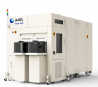
Oriental Crystal Source's new generation of DR-SEM EOS uses an electronic optical design that is compatible with self-developed multi-channel high-speed detectors and supports multi-signal type analysis and detection. It is compatible with EDX component analysis functions and can cover a wide range of defect re-inspection application scenarios. In addition, the new generation of DR-SEM EOS is equipped with high-precision positioning technology, and its detection accuracy and speed can match the mainstream level in the industry.
Next Generation CD-SEM EOS
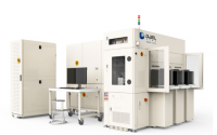
As a benchmark equipment for production line measurement, CD-SEM has core technical requirements for EOS, such as high resolution, high throughput, and high stability. In order to achieve high imaging resolution and high measurement accuracy, Oriental Jingyuan's new generation of CD-SEM EOS adopts new solutions such as spherical chromatic aberration-optimized objective lenses, aberration compensation technology, and automatic correction technology, which have now reached the industry's first-class level.
Next Generation EBI EOS
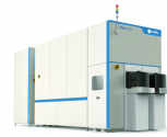
In response to the production line inspection needs of leading domestic logic and storage customers, EBI EOS must focus on improving the inspection speed while ensuring the inspection accuracy. The newly developed EBI EOS by Oriental Jingyuan has made significant optimization and improvement in inspection accuracy and speed through four major technical means. (1) Ultra-large beam current electron beam pre-scanning technology and large-range electron yield adjustment technology meet the diversified inspection needs of different products; (2) Compatible with step-by-step and continuous scanning modes, providing competitive production capacity indicators; (3) Adopting the industry-leading high-speed large beam current inspection solution, the sampling rate reaches the industry advanced level; (4) Immersion electron gun supports a larger beam current adjustment range.
Jingzhou Equipment Completes Tens of Millions of Yuan in Series B Financing
According to MultiGo Capital, Suzhou Jingzhou Equipment Technology Co., Ltd. (hereinafter referred to as "Jingzhou Equipment") recently completed a B round of financing of tens of millions of yuan, jointly invested by MultiGo Capital and various industry parties. This is another important layout of MultiGo in the field of key front-end wet process equipment for pan-semiconductors.
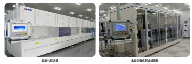
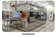
It is reported that Suzhou Jingzhou Equipment Technology Co., Ltd. is an advanced manufacturing enterprise integrating process development, design, manufacturing, sales and after-sales. It provides high-end wet process equipment and process technology for the three major fields of flat panel displays, photovoltaics, and semiconductors. The main products include high-precision cleaning, coating, developing, etching, stripping and other equipment, and simultaneously extend supporting technical services such as intelligent data, green and low-carbon, and products such as online waste liquid recovery systems, intelligent integration and data analysis.
According to Zhongxing Capital, Jingzhou Equipment is the only manufacturer in China that has the ability to supply large-size whole-line wet process. It has made breakthroughs in many national key equipment projects, and its current performance has further exploded. Over the past 10 years, Jingzhou Equipment has accumulated deep pan-semiconductor wet process technology. It entered the G2.5 generation line in 2012, broke through etching and stripping in 2016, broke through development in 2020, and fully mass-produced the 8.6 generation line in 2024. It has conquered key wet process equipment one by one, especially in the national major project large-size Array segment yellow light coating Track line, HF cleaning and other links. It has achieved the industry's first breakthrough. The company's performance in 24 years has further exploded with the expansion of display production. It is currently the main supplier of the industry's leading manufacturers. In the future, its penetration is expected to continue to expand and completely replace German, Japanese and Korean equipment.
Automated Semiconductor Wafer Wet Processing Equipment and Automated Wafer Plating tools.
