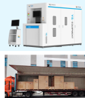
Honglei Optics received an order for a glass substrate (TGV)(Through Glass Vias) direct writing lithography machine
With its advanced lithography technology solutions and professional and efficient team, Honglei Optics has won the favor of important domestic customers in the glass substrate ( TGV ) industry and obtained a purchase order for direct writing lithography machines. The signing of this order marks that our company has taken the lead in entering the field of glass substrate lithography.
Glass substrates are superior to organic substrates in terms of thermal expansion coefficient, signal transmission loss, chemical stability, and wiring density. They are particularly suitable for applications in AI computing chip packaging, C PO optical modules, Mini -LEDs , and other fields. With the continuous optimization of TGV technology and process technology, they are expected to replace organic substrates and become the core substrate in the field of advanced semiconductor packaging.
This time, Honglai Optics has reached an important cooperation with a key manufacturer in the field of glass substrates, marking another important layout of our company in the field of semiconductor advanced packaging lithography.
Honglei Optics is committed to micro-nano direct write lithography solutions. As of now , the company has launched three micro-nano direct write lithography equipment to the market (models: HL P20, HL P6 - E1 , HL P3 -E1 ) , focusing on three application areas: PCB HDI&FPC circuit boards, semiconductor glass substrates, and advanced packaging mask plates, and has obtained orders from leading customers.
The product series planned and developed by the company covers micro-nano direct-write lithography equipment with optical resolution ranging from 20μm to 0.5μm, which can meet the direct-write lithography needs in multiple fields such as PCB HDI&FPC, IC packaging substrates, semiconductor masks, glass substrates and advanced packaging.


