Chinese semiconductor thread II

tokenanalyst

Lieutenant General
Registered Member

Interference-governed electromagnetic-thermal coupling and heat transport in pulse EUV-irradiated multilayer nanofilms​


Mo-Si multilayer mirrors are central to extreme ultraviolet lithography, where nanoscale optical interference and heat accumulation together constrain reflectivity and operational stability. Here we develop an analytical electromagnetic-thermal coupling model that directly links transfer-matrix-based interference-controlled energy deposition with transient heat conduction in EUV-irradiated multilayers. The model reveals a fundamental trade-off whereby increasing the multilayer period number enhances reflectivity but simultaneously elevates temperature by impeding heat dissipation. Interference-driven volumetric absorption further gives rise to pronounced axial temperature gradients and a post-pulse downward migration of the heat-flux maximum, a delayed-heating effect inaccessible to conventional surface-flux-based models. Systematic analysis establishes scaling laws connecting interfacial thermal resistance, beam size, and incident energy density to thermal confinement and temperature rise. By incorporating interfacial compaction kinetics, the model enables a quantitative assessment of mirror lifetime. This work offers a theoretical tool for thermal-optical co-design of multilayer nanostructures including EUV mirrors under pulsed irradiation across a wide spectral range.

Please, Log in or Register to view URLs content!
 

tokenanalyst

Lieutenant General
Registered Member

Yongjiang Laboratory Breaks Through in Ultra-Thin Large Silicon Carbide Wafer Fabrication


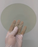
In a major advancement for China’s third-generation semiconductor industry, the Heterogeneous Integration Research Center at Yongjiang Laboratory has successfully developed a novel process to fabricate 6–8 inch, ultra-thin silicon carbide (SiC) wafers as thin as 20–30 micrometers, with exceptional thickness uniformity (TTV < 2 µm) reaching industry-leading standards.

Addressing key industry challenges SiC’s extreme hardness, warping/breakage risks, and thickness control difficulties the team invented a room-temperature, ultra-flat temporary bonding + precision thinning technology, integrated with laser lift-off, replacing traditional high-temperature mechanical grinding. This innovation eliminates thermal stress, dramatically improving yield and precision.
1770045519238.png
The breakthrough enables stable production of high-quality, structurally intact ultra-thin SiC wafers, critical for next-gen applications requiring higher power density, superior heat dissipation, and enhanced high-frequency performance such as high-power semiconductor chips and military phased array radars.

Leveraging its core technology platform, the team rapidly transitioned from R&D to industrial-scale production, significantly shortening the path to market. Next steps include:​
  • Scaling up stable mass production of 6–8 inch wafers​
  • Conducting long-term reliability testing​
  • Optimizing integration with downstream device manufacturing​
  • Initiating pre-research on 12-inch ultra-thin SiC wafer processing
  • Building a robust raw material supply chain and full-process quality control system​
This milestone marks a critical step toward China’s independent control of high-end SiC substrate technology, accelerating the domestic semiconductor industry’s upgrade and global competitiveness.

Please, Log in or Register to view URLs content!
 

tokenanalyst

Lieutenant General
Registered Member

Chenxian Optoelectronics' capacity expansion has attracted attention; a list of its recent winning bids for glass-based Micro LED production line equipment is provided.​


Chenxian Optoelectronics (Chengdu Chenguangdian Co., Ltd.) is expanding its glass-based Micro LED production line in Chengdu High-tech Zone with a 3 billion yuan investment. The project, approved by local authorities, will add 22,000 m² of annual screen production capacity (totaling 40,000 m² after completion) by purchasing over 130 equipment sets.

Key equipment suppliers include:​
  • Suzhou Jiazhicai: Screen aging systems​
  • Hefei Xinyihua: Automated handling, repair machines, and loading/unloading systems​
  • Suzhou Protech: Automated handling systems​
  • Jiangsu Fulat: Grinder and chemical gold plating equipment​
  • Shenzhen Han's: Selective laser transfer systems​
Established in 2020 with a 1.2 billion yuan total investment, the company is backed by Chengdu High-tech Investment Group, Visionox (15.43% stake), and others. It aims to become a leading Chinese Micro LED technology developer. Recent bids (2025–2026) highlight strong domestic equipment supplier participation.
.
Please, Log in or Register to view URLs content!
 

tokenanalyst

Lieutenant General
Registered Member

High-power spectral and polarization modulation coatings for long-wave infrared laser systems​


New-generation semiconductor manufacturing technologies, such as extreme ultraviolet lithography and laser spike annealing, have created an urgent demand for high-power CO₂ laser systems. The 10.6 μm infrared polarization coatings, as a core optical component in these systems, plays a critical role in beam shaping, polarization control, and high-efficiency transmission. However, existing infrared polarization coatings still face numerous challenges in terms of spectral efficiency, polarization characteristics, and laser-induced damage resistance. These challenges severely limit the widespread application of infrared polarization coatings in key integrated circuit equipment. Therefore, this paper systematically investigates the material properties, design methods, fabrication processes, and performance characterization of long-wave infrared polarization coatings, aiming to break through existing technical bottlenecks and enhance the comprehensive performance of infrared polarization coatings to meet the application requirements of high-power CO₂ laser systems in the field of key integrated circuit equipment.​

Please, Log in or Register to view URLs content!
 

tokenanalyst

Lieutenant General
Registered Member

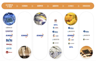
SMIC establishes Advanced Packaging Research Institute​


SMIC's Advanced Packaging Research Institute was officially inaugurated at its Shanghai headquarters. Chen Jie, Standing Committee Member of the Shanghai Municipal Committee and Vice Mayor of Shanghai, and Liu Xunfeng, Chairman of SMIC, jointly completed the ceremony. Officials from the Ministry of Industry and Information Technology and the Shanghai Municipal Government, as well as expert teams from Tsinghua University and Fudan University, were all present. This high-profile event marks a crucial step in the shift from fragmented R&D to collaborative problem-solving in China's advanced packaging field, and is also a core move by SMIC to complete its industrial ecosystem and overcome technological bottlenecks. In his speech, Liu Xunfeng clarified that the institute will focus on cutting-edge advanced packaging technologies and common industry challenges, collaborating with top universities and industry chain partners to build an integrated platform of government, industry, academia, research, and application, creating a leading domestic and internationally advanced R&D and collaborative innovation alliance to precisely address core shortcomings in the industry.

1770065710290.png

Advanced packaging equipment is similar to front-end wafer manufacturing equipment, and suppliers benefit from the growth of the advanced packaging and testing industry. With the development of advanced packaging, new connection methods such as bumping, flipping, TSV, and RDL (rewiring) require increasingly sophisticated equipment. Taking long ball bumps as an example, the main process flow includes pre-cleaning, UBM, deposition, photolithography, solder plating, resist removal, etching, cleaning, and inspection. Therefore, the required equipment includes cleaning machines, PVD equipment, photolithography machines, etching machines, electroplating equipment, and cleaning machines. Materials required include photoresist, developer, etching solution, and cleaning solution. To promote industry development and facilitate resource sharing, we welcome upstream and downstream players in the chip design, wafer manufacturing, equipment, and materials industries to join the Aibang Semiconductor Advanced Packaging Industry Chain Exchange Group.​

Please, Log in or Register to view URLs content!
 

tokenanalyst

Lieutenant General
Registered Member

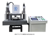
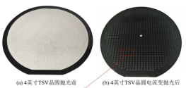
World's first TSV/TGV polishing solution: electrorheological polishing technology​


Guangzhou Zhiyan Semiconductor Equipment Co., Ltd. has unveiled the world’s first electrorheological (ER) polishing technology for Through-Silicon Vias (TSV) and Through-Glass Vias (TGV) key enablers of 3D chip packaging. As Moore's Law faces physical limits, TSV/TGV technologies are critical for improving chip performance through vertical interconnects, but their manufacturing is hampered by costly and complex chemical mechanical polishing (CMP) processes.

Traditional CMP relies on chemical reactions and mechanical grinding to planarize wafers, requiring expensive imported consumables (slurries, pads), high equipment costs, poor process control, and risk of damaging underlying insulating layers.

Zhiyan Semiconductor has developed a novel ER-based polishing method that uses an electric field to dynamically change the viscosity of electrorheological fluid—transforming it from liquid to a solid-like state under high field strength. This creates a controllable, flexible "grinding head" for precise material removal.​
  • Selective Polishing: By adjusting the electric field strength (e.g., conductor below electrode = strong field/high efficiency; insulator below = weak field/low efficiency), the system selectively removes metal layers while protecting insulating materials.​
  • No complex sensors or controls needed—reducing costs and improving reliability.​
  • Low stress polishing: Ideal for ultra-thin wafers.​
  • Flexible design: Enables small-area, localized polishing for precise defect removal.​
  • Full IP ownership: All core materials, equipment, and processes are independently developed by Zhiyan.​
1770073745745.png1770073764931.png
Key Advantages:
-Higher precision & selectivity
-Lower cost and reduced reliance on imported parts
-Better process control and reliability
-Scalable to 4-inch, 6-inch, and 8-inch wafers

This innovation marks a significant step forward in advanced packaging technology, offering a more efficient, sustainable, and affordable alternative to traditional CMP potentially reshaping the future of semiconductor manufacturing.

Please, Log in or Register to view URLs content!
 

tokenanalyst

Lieutenant General
Registered Member

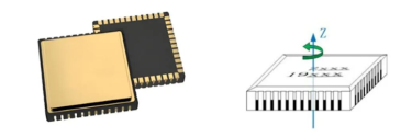
Micro-Magic launches tactical-grade MEMS gyroscope to enhance motion sensing in unmanned autonomous systems.​


Micro-Magic, a leading Chinese inertial sensor manufacturer, has launched a new series of tactical-grade single-axis MEMS gyroscopes (including MG-101/102, MG-401, MG-501, MG-2001, and MG-4001/4002) designed for advanced motion sensing in unmanned autonomous systems. These compact (10mm × 10mm × 3.5mm), lightweight (1.5g) devices feature an all-digital output and a unified ceramic package, enabling high precision and wide dynamic range performance. The sensors support extreme angular rates up to ±4000°/s (for agile applications like racing drones) and stable low-rate measurements down to ±100°/s for long-term underwater operations. Optimized for UAVs, UGVs, USVs, UUVs, and robots, they provide reliable data in harsh environments with vibration and shock. The launch supports the development of smarter, swarming, and more autonomous unmanned platforms, emphasizing the growing importance of high-performance sensor technology in next-generation robotics and defense systems.

About Micro-Magic

Micro-Magic is a leading Chinese inertial sensor designer and manufacturer, offering a wide range of high-quality, cost-effective industrial, tactical, and navigation-grade inertial sensors, such as quartz flexure accelerometers, fiber optic gyroscopes, inertial measurement units (IMUs), inertial navigation systems (INS), compasses (including MEMS and FOG-based models), and inclinometers/tilt meters. Micro-Magic also supports customized inertial sensor product designs based on customer needs.

1770073919339.png

Please, Log in or Register to view URLs content!
 

huemens

Junior Member
Registered Member
Digitimes is reporting that YMTC has entered LPDDR5 sampling stage. They also claim half of the new Phase 3 fab will be allocated for DRAM.

YMTC makes its "first foray into cross-industry" by sending out LPDDR5 engineering samples​

Please, Log in or Register to view URLs content!
Supply chain sources also revealed that Yangtze Memory Technologies Co., Ltd. (YMTC) is no longer content with merely being China's leading player in 3D NAND. It has recently quietly entered the DRAM and HBM (High Bandwidth Memory) technology fields, having already completed the development of LPDDR5 engineering samples. Its new Phase III plant in Wuhan, expected to start production in the second half of 2026, has recently been topped out, with DRAM as its primary focus for capacity expansion. Driven by both capacity expansion and policy mandates, YMTC is expected to reshape the global memory landscape.
It is understood that Yangtze Memory Technologies Co., Ltd. (YMTC) has adopted a low-key "duck paddling" strategy, and has carried out DRAM R&D processes internally ahead of schedule. The Wuhan Phase III project will allocate production capacity with DRAM and NAND each accounting for about half, becoming YMTC's first DRAM production base.
 

gotodistance

New Member
Registered Member
YMTC judged the situation as a "golden time." According to industry sources, YMTC is not just selling NAND products but is also seeking to supply solutions in the form of a multi-chip package (uMCP) combining NAND flash and DRAM. Its strategy is to replace the vacancy of Samsung Electronics and SK Hynix by targeting the NAND+ DRAM package market, which smartphone manufacturers prefer for space efficiency.

YMTC는 이 상황을 '골든 타임'으로 판단했다. 업계에 따르면 YMTC는 단순히 낸드 단품 판매에 그치지 않고, 자사의 낸드플래시와 D램을 결합한 멀티칩 패키지(uMCP) 형태의 솔루션 공급을 추진 중인 것으로 알려졌다. 스마트폰 제조사들이 공간 효율을 위해 선호하는 낸드+D램 패키지 시장을 공략함으로써, 삼성전자와 SK하이닉스의 빈자리를 대체하겠다는 전략이다.

Please, Log in or Register to view URLs content!
 

sunnymaxi

Colonel
Registered Member
Japanese news outlet AsiaNikkei too reporting the same information.

Massive expansion in memory production from both CXMT and YMTC.

1. CXMT is the world’s fourth-largest DRAM maker following Samsung Electronics, SK Hynix, and Micron (with a market share of approximately 11.1% based on production capacity), which could expand to about 13.9% by 2027.

2. YMTC’s NAND market share could expand from about 12% in 2025 to 15% by 2028.

Please, Log in or Register to view URLs content!
 
Top