Chinese semiconductor thread II

tokenanalyst

Brigadier
Registered Member

Jingce Electronics: Products have completed 7nm advanced process delivery, and more advanced process products are being verified​

Jingce Electronics stated on its investor interaction platform that some of the company's main products have completed the delivery and acceptance of 7nm advanced process, and products with more advanced processes are currently being verified.

Jingce Electronics is one of the leading companies in the field of semiconductor testing equipment in China. It has basically formed a layout in the entire field of front-end and back-end semiconductor testing. The company's subsidiary Wuhan Jinghong mainly focuses on the field of automatic test equipment (ATE) (the main product is memory chip testing equipment). The aging (Burn-In) product line has achieved batch repeat orders from domestic first-line customers, and the CP (Chip Probe)/FT (Final Test, i.e. factory test) product line related products have obtained corresponding orders and completed delivery.

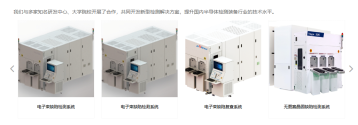
It is reported that Shanghai Jingce's core products such as film thickness series products, OCD equipment, electron beam equipment, semiconductor silicon wafer stress measurement equipment, and bright field optical defect detection equipment are all in the leading position in the domestic industry, with obvious competitive advantages. Since the beginning of this year, the proportion of Jingce Electronics' advanced process products in the company's overall revenue and orders has continued to increase, and it is expected to become the core support point of the company's performance in the future.
1753885865154.png

Please, Log in or Register to view URLs content!
 

tokenanalyst

Brigadier
Registered Member
Interesting

From FinFET to Flip FET: China's solution for three-dimensional transistors emerges​


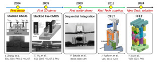
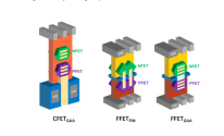
At the 2025 VLSI Symposium, a team from Peking University introduced Flip FET (FFET), a revolutionary 3D transistor architecture poised to redefine semiconductor scaling. This innovation achieves 8-layer vertical stacking, boosting logic density by 3.2x and cutting power consumption by 58% compared to traditional FinFETs. Flip FET is hailed as a leading contender to sustain Moore’s Law beyond the 1nm node, offering a homegrown Chinese solution to global chipmaking challenges.

1753886190551.png
  1. Architecture:​
    • Stacks front-side nFETs (NFETs) and back-side pFETs (PFETs) via wafer flipping, enabling double-sided active devices.​
    • Combines backside power rails (BPR) and double-sided interconnects to slash power resistance by 40% and improve voltage stability.​
    • Achieves a natural split-gate design and multi-threshold voltage tunability (~500 mV), enhancing design flexibility.​
  2. Performance Breakthroughs:​
    • Back-side PFETs match front-side NFETs in performance: SS = 73.1 mV/dec, DIBL = 24 mV, and on/off ratio of 10⁷.​
    • Enables ultra-dense logic cells (<5T height) and SRAM scaling at the A2 node, validating its potential for sub-1nm nodes.​
  3. Manufacturing Edge:​
    • Built using non-EUV lithography, compatible with 7nm production lines in China.​
    • Leverages existing tools for wafer bonding, thinning, and alignment, reducing industrialization barriers.​

-vs. FinFET/GAA:​
  • FinFETs (used in 16nm–5nm nodes) and GAA (3nm/2nm) face scaling limits due to leakage and process complexity.​
  • Flip FET’s 8-layer stacking and double-sided design outperform GAA in density and power efficiency.​
-vs. CFET (IMEC’s Roadmap):
  • CFET stacks n/p transistors vertically but requires complex EUV-dependent processes.
  • Flip FET’s double-sided separation improves power efficiency and scalability for ultra-dense chips.
  • FFET fully leverages the current equipment landscape in mainland China, is compatible with existing production lines, and utilizes a non-EUV-reliant process. Industry insiders reveal that it can be fabricated on a 7nm process, leveraging mature equipment and effectively lowering the barrier to industrialization. This integration approach leverages existing lithography technology and design capabilities to continuously increase the integration density of integrated circuits, making it more adaptable to the current state of China's domestic industrial chain.
1753886233357.png

Please, Log in or Register to view URLs content!
 
Last edited:

tokenanalyst

Brigadier
Registered Member

Hualin Jiaye | Breaking through technical barriers! CGB successfully delivers 12-inch fully automatic tank cleaning equipment.​


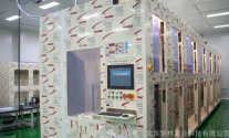
In this crucial year for the localization of semiconductor equipment, Beijing Hualin Jiaye Technology Co., Ltd. (CGB) has achieved another success: its independently developed 12-inch fully automatic tank cleaning system has been officially delivered to a top five domestic semiconductor equipment company. This milestone not only demonstrates CGB's technological strength in semiconductor wet process equipment, but also provides strong equipment support for the independent and controllable development of my country's third-generation semiconductor industry chain.

1753886468226.png

Beijing Hualin Jiaye Technology Co., Ltd. , a leading domestic manufacturer of professional semiconductor equipment, specializes in the research, development, and production of wafer cleaning, drying, and surface treatment technologies. Headquartered in the Beijing Yizhuang Economic and Technological Development Zone, the company maintains a northern production base in Langfang, Hebei, and an East China regional service center in Wuxi. CGB also has an R&D center in Japan, focusing on product development and overseas market services.

Product application areas include: integrated circuits (ICs), microelectromechanical systems (MEMS), silicon materials (Si), compound semiconductors, optical communication devices, power devices, semiconductor lighting (LEDs), advanced packaging, photovoltaic cells, flat panel displays (FPDs) and scientific research (R&D), etc.

As a domestic manufacturer of semiconductor wet process equipment, fully automatic wafer chamfering machines, fully automatic wafer brushing machines, dryers, chemical supply systems and other equipment, CGB always strictly follows international quality management system standards to conduct all-round and full-process quality control, while focusing on continuous improvement and innovation.

Please, Log in or Register to view URLs content!
 

tokenanalyst

Brigadier
Registered Member

Shuoke Crystal's annual production of 1 million mm silicon carbide single crystal project has officially started!​


On July 30, the launching ceremony of the 1 million mm/year silicon carbide single crystal project of Shanxi Shuoke Crystal Co., Ltd., a subsidiary of China Electronics Technology Group Corporation Semiconductor Materials Co., Ltd., was held in Taiyuan City, Shanxi Province.

The 1 million mm annual output silicon carbide single crystal project is a model of central-local cooperation strategically built by China Electronics Technology Group Corporation and the People's Government of Shanxi Province. It aims to gather innovative forces, drive the upstream and downstream of the industrial chain, and build a domestic leading silicon carbide single crystal growth industrial base. After it is put into production, it will add 1 million mm silicon carbide single crystals and 300,000 silicon carbide substrates production capacity, and quickly realize the industrialization of 8-inch silicon carbide substrates and the engineering application of 12-inch silicon carbide substrates.

Please, Log in or Register to view URLs content!
 

tokenanalyst

Brigadier
Registered Member

Shandong Liguan launches large-scale PVT equipment, a breakthrough in domestic silicon carbide equipment​


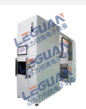
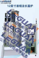
Recently, #ShandongLiGuan officially launched its 12-inch PVT resistor equipment and 8-inch multi-crucible equipment, setting a new industry benchmark for the large-scale, stable and low-cost preparation of 8-12 inch SiC wafers.

The 12-inch PVT resistor equipment and 8-inch multi-crucible equipment released by Shandong Liguan are core process equipment for the preparation of silicon carbide wafers. They can determine the growth efficiency, quality and cost of silicon carbide ingots, and are closely related to the development of the silicon carbide industry.

It is understood that the single-furnace growth efficiency of the 12-inch PVT resistance furnace has been increased by 40%, and it integrates advanced multi-temperature zone precision control technology, which can effectively ensure the lattice quality and thickness consistency, and can meet the stringent mass production quality requirements.

1753887598693.png

The 8-inch multi-crucible equipment utilizes 3-5 crucibles for synchronous growth, doubling single-shot output and significantly reducing ingot manufacturing costs. Furthermore, its innovative hardware architecture, integrated with intelligent control software, enables high-precision dynamic temperature and vacuum pressure control. Its unique multi-crucible coordinated temperature field technology also solves the uneven thermal field distribution problem of traditional oversized equipment.

1753887670242.png

Please, Log in or Register to view URLs content!
 

Nevermore

Junior Member
Registered Member
Please, Log in or Register to view URLs content!

The Cyberspace Administration of China summoned Nvidia regarding the backdoor security risks of its H20 computing chip vulnerabilities.

[The Cyberspace Administration of China summoned Nvidia regarding the security risks of a backdoor vulnerability in its H20 computing chip] Cailianshe reported on July 31st that serious security issues with Nvidia's computing chips have recently been exposed. Previously, US lawmakers called for advanced chips exported from the US to be equipped with "tracking and positioning" capabilities. US artificial intelligence experts revealed that Nvidia's computing chips have mature "tracking and positioning" and "remote shutdown" technologies. To safeguard the network and data security of Chinese users, and in accordance with the relevant provisions of the Cybersecurity Law, the Data Security Law, and the Personal Information Protection Law, the Cyberspace Administration of China summoned Nvidia on July 31, 2025, requesting that the company explain the security risks of a backdoor vulnerability in its H20 computing chips sold to China and submit relevant supporting documentation.
 

Overbom

Brigadier
Registered Member
Edit: Seems someone just posted this also. Scmp is light on details

questions for H-20 backdoor
Please, Log in or Register to view URLs content!

Breaking | China’s cyberspace regulator summons Nvidia to explain H20 chip’s alleged ‘back door’ risks​

China’s cyberspace regulator has summoned Nvidia to explain the security risks related to the so-called “back door safety” of its H20 chips, according to a statement on its website.

The Cyberspace Administration of China said it has summoned and interviewed Nvidia over the tracking and remote control risks of its H20 chips and has requested the US company to explain and provide relevant proof regarding the issue.
 

BlackWindMnt

Major
Registered Member
Edit: Seems someone just posted this also. Scmp is light on details

questions for H-20 backdoor
Please, Log in or Register to view URLs content!

Breaking | China’s cyberspace regulator summons Nvidia to explain H20 chip’s alleged ‘back door’ risks​

Sounds like china is applying some light lawfare to make nvidia less attractive to buy.
 

Overbom

Brigadier
Registered Member
Sounds like china is applying some light lawfare to make nvidia less attractive to buy.
I mean it's meaningless. If they just "ask", NVIDIA can say whatever bs and pinky promise or misdirect etc

Nothing else than full deep technical hardware and software inspection would be enough to confirm that nothing shady is going on
 
Top