Chinese semiconductor thread II

european_guy

Junior Member
Registered Member
Huawei controls the whole stack. So they have no reason to continue paying royalties to ARM I think.

Paying royalties to ARM is the least reason for HW to switch architecture. Supply chain reliability and geopolitical uncertainty are definitely much higher priorities in the decision process.

Because both ARM and RISC-V are
Please, Log in or Register to view URLs content!
, the actual CPU migration mainly involves updating the CPU subsystem called "instruction decoder", so the biggest effort is not in the hardware, but in porting the large software ecosystem around the CPU. This is a huge task!

I expect HW will seriously start moving away from ARM, only once the new
Please, Log in or Register to view URLs content!
will be stabilized (1 year at least). Rumors say issues with Harmony OS NEXT seem the reason of the few-months delay of the new Mate 70. It's OK, this is a big update: Harmony OS NEXT is going to ditch old Android code altogether, not a small thing. Actually it is already an impressive achievement if only few months of delay occur.
 

tokenanalyst

Brigadier
Registered Member

SAIC Motor and ZTE signed a strategic cooperation agreement to expand the scope of cooperation to 5G communication modules, etc.​


On August 20 , SAIC Motor and ZTE held a press conference for the launch of the global platform of China's largest automotive cloud communication product. At the same time, the two parties signed a strategic cooperation agreement. The two parties will rely on their respective advantages to carry out in-depth cooperation in multiple fields. The scope of cooperation will be further expanded from 4G to 5G communication modules, automotive operating system software, computing power construction and large models and other innovative technology fields. In addition, it will also expand horizontally to digital transformation, corporate development strategy and R&D management, internationalization and compliance management systems.

Please, Log in or Register to view URLs content!
 

tokenanalyst

Brigadier
Registered Member

The Institute of Microelectronics has made new progress in in-sense computing​

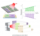
With the rapid development of artificial intelligence technology, the surge in sensor data has posed severe challenges to data processing speed and energy efficiency. Traditional sensor architectures (such as the von Neumann architecture) physically separate sensing, computing, and storage units, and their large amounts of data conversion and transmission further increase energy consumption and time delays. To meet this challenge, researchers have proposed an advanced sensor architecture, in-sense computing technology, which can simultaneously perceive and process images at the sensor level. Organic semiconductors have attracted much attention due to their intrinsic flexibility and adjustable band gap, especially in near-infrared (NIR) optoelectronic applications, which have great potential applications such as fluorescence imaging, medical monitoring, remote sensing, and optical communications. However, organic optoelectronic devices still face huge challenges in realizing intelligent sensing, especially in-sense computing.

Recently, the team of Academician Liu Ming/Researcher Li Mengmeng from the Institute of Microelectronics has developed a new heterojunction structure composed of partially overlapping p-type and n-type organic semiconductor materials. The structure can be processed using conventional photolithography technology and can achieve an integration density of up to 520 devices per square centimeter and a channel length of 5 microns. The heterojunction uses the light gating effect to achieve positive and negative responses to near-infrared light (>1000 nm). More importantly, the photoresponsivity of the heterojunction is linearly related to the gate voltage, and real-time matrix multiplication operations can be performed in the sensor, realizing efficient and accurate near-infrared sensor computing functions including image processing and non-destructive reading and classification, providing new routes and new ideas for the development and application of organic electronics in the next generation of intelligent sensory systems.

This work was supported by the National Key R&D Program and the National Natural Science Foundation of China. The research results were published in the recent Advanced Materials under the title " Gate-Tunable Positive and Negative Photoconductance in Near-Infrared Organic Heterostructures for in-Sensor Computing ", and were selected as Editors' Choice highlights and as the inside back cover of the journal . Xu Yunqi, a graduate student at the Institute of Microelectronics, is the first author of the paper, and Li Mengmeng, a researcher at the Institute of Microelectronics, is the corresponding author.

1724165469222.png


Please, Log in or Register to view URLs content!
 

tokenanalyst

Brigadier
Registered Member

Aisen Semiconductors: the revenue from photoresist and supporting reagents continued to increase.​


Revenue from photoresist and supporting reagents continues to increase, and small-batch orders have been obtained for electroplating tin-silver additives for advanced packaging: In terms of business, in the first half of 2024, 1) the company's sales revenue from electroplating solution and supporting reagents was 83.45 million yuan, an increase of 13.31% over the same period last year, and the main business revenue accounted for 46.47%. ① In the field of advanced packaging, electroplating tin-silver additives have passed the certification of Changdian Technology and obtained small-batch orders, and electroplating copper base solution (high-purity copper sulfate) has been officially supplied to Huatian Technology.

Electroplating copper additives are in batch stability verification. ② In the wafer field, the copper plating additive products for the 28nm Damascus copper interconnection process have entered the sample trial production and product certification stage; the ultra-high purity cobalt sulfate for the 14nm advanced process has completed sample production, and the client test is progressing smoothly; the cleaning liquid for the wafer manufacturing copper process has completed customer testing and certification, and has achieved small-batch delivery. 2) The sales revenue of photoresist and supporting reagents was 40.83 million yuan, an increase of 44.57% over the same period last year, and the main business revenue accounted for 22.73%. The company took the supporting reagents for photoresist as the entry point and has successfully achieved the large-scale supply of adhesion promoters, developers, removers, etching solutions and other products to downstream packaging manufacturers. At the same time, the company actively carried out the research and development of photoresists, with advanced packaging negative photoresists, OLED array manufacturing photoresists, and PSPI for wafers and other special process photoresists as breakthroughs, covering wafer manufacturing, advanced packaging and semiconductor display and other application fields, successfully breaking the foreign monopoly and gradually extending to advanced processes. At present, the company's self-developed negative photoresist for advanced packaging and positive photoresist for wafer manufacturing i-line have achieved mass supply. 3) Sales revenue of electroplating supporting materials was 55.31 million yuan, an increase of 24.09% over the same period last year, and the main business revenue accounted for 30.80%.

Please, Log in or Register to view URLs content!
 

OptimusLion

New Member
Registered Member
Peking University has made progress in the field of carbon-based FET biosensors to promote their application in POCT

Field effect transistor (FET) biosensors have significant advantages such as high sensitivity, rapid response and label-free detection, and show great potential in the field of medical point-of-care testing (POCT). FETs based on thin film semiconductor materials have advantages such as good process compatibility and excellent gate control characteristics, so they are highly anticipated in biosensor applications. Semiconductor carbon nanotube (CNT) films have been proven to be ideal channel materials for building high-performance FET biosensors. Although a large number of related research works have been published, they have not yet developed into a true engineering technology. The main reason is that there are key technologies to be solved and the complete technology chain of CNT FET biosensors has not yet been developed, which makes carbon-based biosensor research still limited to the laboratory stage.

Recently, Professor Zhang Zhiyong and Assistant Researcher Xiao Mengmeng from the School of Electronics and the Center for Carbon-Based Electronics Research at Peking University have analyzed from the perspective of practical applications that the complete technical chain of large-scale manufacturing of FET biosensors needs to solve at least two major challenges: (i) developing reliable and scalable manufacturing methods to obtain consistency between batches, and (ii) realizing reliable methods for reading weak signals and portable terminal systems that can read packaged sensor chips. Overcoming these challenges and building a complete technical chain is the basis for promoting the engineering of FET biosensors and, in turn, their application in the field of POCT.

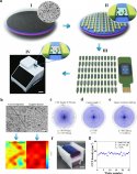
The Peking University team solved the technical difficulties of CNT material preparation, biosensor manufacturing, chip packaging and signal reading point by point, creating a complete chain technology of CNT FET biosensors and developing a solid technical foundation for its application in the field of POCT. Specifically, in terms of material preparation, high-quality and uniform randomly oriented semiconductor CNT films were prepared by improved dip coating technology (Figure 1).
1440036398676.4382.jpeg


Figure 1: The complete technology chain of CNT FET biosensor

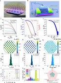
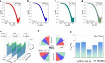
In device preparation, by optimizing the preparation process of CNT FET biosensors, batch preparation of 4-inch wafer carbon-based FETs has been achieved, and the device uniformity has been greatly improved. The coefficient of variation of device performance within the wafer is better than 6%, and the coefficient of variation of device performance between wafers is within 9% (Figures 2 and 3).
63365879866.11918.jpeg

Figure 2: Electrical characteristics of CNT FETs fabricated using standard photolithography
1373074381048.4019.jpeg

Figure 3: Wafer-to-wafer uniformity of CNT FETs
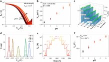
The research team further verified the repeatability of the CNT FET-based ion sensor. At each fixed ion concentration, the standard deviation of the threshold voltage of the tested sensors (100) was within 5.1 mV, which means that the ion concentration information of the solution to be tested can be read by directly testing the drain current of the sensor (Figure 4).
1707657438026.2532.jpeg

Figure 4: Performance of CNT FET ion sensor
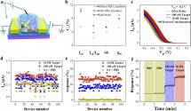
On this basis, the research group developed a standard process for CNT FET biosensor dicing and packaging, and specially developed a dedicated portable device for FET biosensor signal readout, which can realize the plug-and-play of biosensor chips, with a friendly operation interface, and non-professionals can also detect biological targets according to simple instructions. The research group also demonstrated that through this portable and efficient detection system, the detection method and data processing method are optimized, and the CNT FET biosensor can detect biological signals with a concentration as low as 100 aM under a blank background (Figure 5).
1354877227192.3225.jpeg

Figure 5: Performance of CNT FET biosensor
This work has opened up the complete technical chain of carbon-based FET biosensors, laying a technical foundation for promoting their application in the field of POCT. The relevant results were published online in the journal Nano Letters on August 15 in a paper titled "Mass Production of Carbon Nanotube Transistor Biosensors for Point-of-Care Tests". Liu Haiyang, a 2021 doctoral student at the School of Electronics of Peking University, is the first author of the paper. Assistant Researcher Xiao Mengmeng and Professor Zhang Zhiyong from the School of Electronics of Peking University and the Center for Carbon-Based Electronics Research are co-corresponding authors. Dr. He Jianping from the Hunan Advanced Sensing and Information Technology Innovation Research Institute of Xiangtan University and others participated in this work as co-authors.
This work was supported by the National Key R&D Program of China (No. 2022YFB3204402), the National Natural Science Foundation of China (No. 62225101 and 62174007), and the Micro-Nano Processing Laboratory of Peking University.
 

tokenanalyst

Brigadier
Registered Member

Will Semiconductor's net profit in the first half of 2024 increased by nearly 800% year-on-year​


The report shows that in the first half of 2024 , Weilan Technology achieved operating income of 12.091 billion yuan, a year-on-year increase of 36.50% ; the net profit attributable to shareholders of listed companies was 1.367 billion yuan, a year-on-year increase of 792.79% ; the non-net profit was 1.372 billion yuan, turning a loss of 78.96 million yuan in the same period last year into a profit.

Regarding the significant year-on-year increase in net profit in the first half of 2024 , Will shares said that this was mainly because as the consumer market further recovered, downstream customer demand increased, and with the company's product introduction in the high-end smartphone market and the continued penetration of autonomous driving applications in the automotive market, operating income achieved a significant increase. At the same time, affected by factors such as product structure optimization and cost control, the company's product gross profit margin gradually recovered, and the comprehensive gross profit margin during the reporting period was 29.14% , an increase of 8.21 percentage points year-on-year.

Please, Log in or Register to view URLs content!
 

tokenanalyst

Brigadier
Registered Member

Benefiting from the industry recovery, GigaDevice's net profit in the first half of the year increased by 53.88% year-on-year​


On August 20, GigaDevice released its 2024 first half performance report, saying that H1 operating income was 3,609,037,320.17 yuan, a year-on-year increase of 21.69%; net profit attributable to shareholders of the listed company was 517,000,013.68 yuan, a year-on-year increase of 53.88%; net profit attributable to shareholders of the listed company after deducting non-recurring gains and losses was 473,449,975.7 yuan, a year-on-year increase of 71.87%. Net cash flow from operating activities was 1,248,715,713.3 yuan, a year-on-year increase of 93.73%.

Among them, during the reporting period, operating income increased by 21.69% year-on-year. The main reasons are: after experiencing sluggish market demand and gradual inventory liquidation in 2023, demand in the consumer and network communication markets rebounded in the first half of 2024, driving the company's storage chip product sales and revenue growth; in terms of operations, the company continued to maintain a market share-centered strategy, continued to invest in research and development and product iterations, and the competitiveness of the company's multiple product lines continued to increase, promoting product sales and revenue growth.

Please, Log in or Register to view URLs content!
 

gelgoog

Lieutenant General
Registered Member
That US report claiming GigaDevice can sell their chips for 20-30% less than STMicro because of "Chinese government subsidies" is just plain hogwash. The reason their devices are cheaper is that instead of having multiple separate chip designs according to the required embedded Flash by the client, GigaDevice uses innovative packaging where the Flash is in a separate die inside the chip package.
Please, Log in or Register to view URLs content!

This means they can more easily adapt to consumer demand and don't need to have as many stockpiles of useless chips. It also means chip fabrication is much simpler, less chip licensing fees need to be paid, less investment into chip design of multiple variants, masks, etc.
 

OptimusLion

New Member
Registered Member
Jita Semiconductor's patent for "MOSFET device based on TDDB optimization and its preparation method" was announced

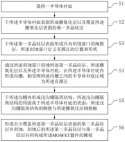
Tianyancha shows that Shanghai Jita Semiconductor Co., Ltd.'s patent for "MOSFET device based on TDDB optimization and its preparation method" was announced, the application publication date is August 9, 2024, and the application publication number is CN118471899A.

img-1724216097404img-973615101142.jpg


The present invention provides a MOSFET device based on TDDB optimization and its preparation method. The present invention uses two polysilicon growth and etching processes to ensure that the thickness of the formed gate oxide layer and the gate electrode meet the corresponding process thickness requirements of the MOSFET device. At the same time, the top surface of the formed shallow trench isolation structure is higher than the surface of the semiconductor substrate, and the side wall of the shallow trench isolation structure is in contact with the gate oxide layer, which can avoid damage to the gate oxide layer at the top corner area of the shallow trench isolation structure during the subsequent etching of the second polysilicon layer, thereby protecting the gate oxide layer at the top corner area of the shallow trench isolation structure, increasing the process thickness of the gate oxide layer at the top corner area of the shallow trench isolation structure, and finally optimizing the reliability of TDDB, so that the MOSFET device has a higher breakdown voltage and a longer reliability life.
 

OptimusLion

New Member
Registered Member
Hejian Software and Open Source Chip Research Institute deepen strategic technical cooperation to enable the construction of large-scale systems of "Xiangshan" high-performance open source RISC-V processors

Shanghai Hejian Industrial Software Group Co., Ltd. (hereinafter referred to as "Hejian Industrial Software") and Beijing Open Source Chip Research Institute (hereinafter referred to as "Open Source Institute") have deepened their strategic technical cooperation on the "Xiangshan" high-performance open source RISC-V processor project, and applied Hejian Industrial Software's commercial-grade full-scenario verification hardware system UniVista Unified Verification Hardware System (hereinafter referred to as "UVHS") to improve the development and verification efficiency of the "Xiangshan" high-performance open source RISC-V processor, promote innovation and accelerate the time to market of next-generation product technologies.

The "Xiangshan" high-performance open source RISC-V processor was developed by the Beijing Open Source Chip Research Institute and quickly became an innovation leader in the RISC-V ecological community. The Xiangshan project aims to promote the development of high-performance open source processors in China. With the help of the RISC-V instruction set architecture (ISA), Xiangshan has developed three generations of processors and has gained wide recognition and respect in the RISC-V community. Its innovative design and high performance make it a reference design for high-performance RISC-V implementations, and it has won many honors at many top international summits.

Hejian Software worked closely with OpenCore Research Institute to successfully apply Hejian Software's full-scenario verification hardware system UVHS in the development of the second-generation "Nanhu" and third-generation "Kunming Lake" processors and the optimization of the software ecosystem, significantly improving development efficiency.

Automatic segmentation technology and clock conversion technology simplify platform migration costs: The flexible scalability of the "Xiangshan" processor requires that large multi-core designs can be segmented onto multiple FPGAs. UVHS's automatic segmentation technology fully automates the entire process, and its powerful clock conversion engine can automatically handle multiple asynchronous clocks within the design, greatly simplifying the manual work of engineers and making it easier to quickly migrate ASIC-style RISC-V RTL code to the FPGA platform. The dual-core RTL code of "Xiangshan" was imported in less than a week to enable Linux OS startup on UVHS.

High operating performance significantly shortens software running time: Based on Xilinx's new FPGA platform, UVHS system's global timing-driven intelligent automatic segmentation technology can push operating performance to a higher level, thereby optimizing the software development project cycle with higher efficiency.

Rich debugging methods: UVHS system supports UHD infinite depth waveform debugging, triggering, asynchronous register readback and other functions, similar to the waveform debugging function of simulation mode, which significantly improves the debugging efficiency and problem location ability. DDR and SRAM backdoor access also greatly increases the convenience of user debugging.

At the same time, UVHS large-scale system cascade can cascade up to tens of billions of logic gates. It has been successfully deployed in many commercial customers, achieving the cascade of up to 160 VU19P FPGAs, meeting the needs of HPC ultra-large system scale verification, and providing reliable technical support for Xiangshan's future RISC-V large-scale system expansion.

On the other hand, UVHS is equipped with a wealth of high-speed interface and storage model solutions, supporting multiple rate adapter solutions such as PCIe Gen5, MIPI CSI2/DSI2, Ethernet 1G-800G, as well as DDR5, DDR4, LPDDR5, LPDDR4, HBM3 and other storage models, which can help users of the RISC-V ecosystem quickly build a complete verification scenario.

Wu Xiaozhong, Vice President of Hejian Software, said: "The Xiangshan processor has made important innovative contributions to the development of the RISC-V ecosystem. We are very proud to support OpenCore Institute through the UVHS hardware acceleration platform to help them accelerate project development and improve design stability. UVHS is an innovative high-performance, large-capacity full-scenario verification hardware acceleration platform designed to cope with today's complex and diverse SoC software and hardware verification tasks. Based on our successful deployment experience in large chip projects of many customers, we look forward to continuing to help the Xiangshan processor achieve project convergence more efficiently in large system design and development, and work with Xiangshan to contribute productivity tools to the RISC-V ecosystem."

Future Directions and Innovations

The cooperation between Hejian Software and OpenCore on the "Xiangshan" project marks an important milestone in the RISC-V ecosystem. By combining the "Xiangshan" innovative processor design with Hejian Software's advanced verification technology, the development of high-performance open source RISC-V processors can be accelerated. At the same time, the cooperation between Hejian Software and OpenCore will further promote innovation in the RISC-V ecosystem:

Multi-core large processor verification

As the multi-core scale and complexity of RISC-V processors increase, the interaction and consistency issues between multiple cores become more complicated, including memory consistency and cache consistency. Verification tools and methods need to be able to execute operations on multiple cores simultaneously and compare expected results to ensure the correctness and performance of multi-core systems in various situations. Hejian Software will further maintain in-depth technical cooperation with OpenCore Institute in this regard.

CPU Debugging Tools

As Xiangshan pushes the limits of RISC-V performance, the complexity of design verification grows exponentially. Ensuring the correctness of advanced features such as out-of-order execution, speculative execution, and complex cache hierarchies requires complex verification methods and tools. General and convenient processor debugging tools can comprehensively analyze, optimize, and verify all stages from single-core to multi-core systems, and can also promote technology and efficiency innovation for the entire ecosystem. Relying on the experience of developing other CPU ecosystems, Hejian Gongsoft will explore and develop new tools in the RISC-V field with OpenCore Institute.

Performance testing and optimization

In order to achieve industry-competitive performance levels, the processor's microarchitecture, bus architecture, and storage performance must be continuously optimized. The entire process requires extensive testing and verification under various workloads and usage scenarios to ensure that the processor system can operate stably and efficiently under different conditions. The hardware platform verification solution provided by Hejian Gongsoft can cover the testing and verification of common application scenarios, while coping with extreme and unexpected operating conditions to ensure the robustness and reliability of the processor.

Ecosystem expansion

The success of the cooperation between Hejian Gongsoft and Xiangshan will attract more partners to join the RISC-V ecosystem. By establishing a strong support ecosystem, including localized documentation, developer portals and application examples, it can promote the application and innovation of RISC-V in various fields. Through these optimizations and corrections, the complexity of current multi-core processor design and verification, as well as the tools and methods required, are more accurately reflected.
 
Top