You are using an out of date browser. It may not display this or other websites correctly.
You should upgrade or use an alternative browser.
You should upgrade or use an alternative browser.
Chinese semiconductor thread II
- Thread starter vincent
- Start date
If 9100 ends up being 5nm in density, then I seriously suspect there have been two different chips. At the beginning of this year there were rumors about a 6nm chip with density that is only slightly higher than 7nm. But, now rumors are that there are 5nm chips, and both Nova 13 and mate 70 are delayed. I suspect plans have changed.these are strange claims.
"reaches the level of TSMC 5nm and has the performance of 8g2" doesn't mean anything.
things that matter are the critical dimensions. And 9000S critical dimensions are so far off N5 that it would be ridiculous to think they can make that jump in 1 improvement.
Could they have chip samples with 140 MMTR/mm2? Sure, but I don't think that's the process for 9100. You'd need a steady production process able to reliably produce 110mm2 die.
Pure speculations, though.
I do think that's not all that relevant. The key here is the chip performance. All the rumors of the x nm and x density is important, but what people truly care about are the power consumption and performance of phone. we will see.If 9100 ends up being 5nm in density, then I seriously suspect there have been two different chips. At the beginning of this year there were rumors about a 6nm chip with density that is only slightly higher than 7nm. But, now rumors are that there are 5nm chips, and both Nova 13 and mate 70 are delayed. I suspect plans have changed.
Pure speculations, though.
Quickie
Colonel
The claim made was about the improvement in the chip performance principally concerning the transistor node improvement, likely in relation to the gate length/contacted area, fin width/height, etc. The claim was not made on improvement in node density though so the assumption could be that the distance between the nodes remains basically the same while the node feature dimension was successfully reduced and improved.If 9100 ends up being 5nm in density, then I seriously suspect there have been two different chips. At the beginning of this year there were rumors about a 6nm chip with density that is only slightly higher than 7nm. But, now rumors are that there are 5nm chips, and both Nova 13 and mate 70 are delayed. I suspect plans have changed.
Pure speculations, though.
6nm means probably TSMC. And you have to remember that the US put restrictions on Chinese imports of GPUs and compute devices above a certain compute power. They hold TSMC over a barrel. Which means these chips will plateau in terms of performance.
AVIC Infrared's new generation compound semiconductor research and development base project starts production line commissioning
Recently, the commissioning and launching ceremony of the production line of the new generation compound semiconductor research and development base project of AVIC Infrared was successfully held in the Lingang New Area of Shanghai. This marks another important milestone in the field of infrared detector technology in my country, and indicates that AVIC Infrared has taken a solid step in promoting independent innovation in infrared detection technology and enhancing international competitiveness.
The project aims to build a domestically leading and world-class infrared detector research and production base, mainly providing a full set of solutions from antimonide wafers to detector imaging components, which will comprehensively enhance my country's independent innovation capabilities in infrared detectors, narrow the technological gap between infrared detectors and foreign countries, and systematically solve the demand for refrigerated detectors for domestic guided weapons and military optoelectronic equipment. After completion, it will have the capacity to produce 10,000 sets of focal plane detectors annually, promote the technological progress of my country's infrared detectors, drive the development of related industries, and create greater economic and social benefits.
Shengmei Shanghai launches Ultra C vac-p panel-level advanced packaging negative pressure cleaning equipment
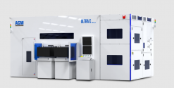
Shanghai ACM Semiconductor Equipment Co., Ltd. (hereinafter referred to as "ACM Shanghai") (Sci-Tech Innovation Board Stock Code: 688082), as a leading supplier of wafer process solutions for semiconductor front-end and advanced wafer-level packaging applications, today launched the Ultra C vac-p negative pressure cleaning equipment for fan-out panel-level packaging applications.

The equipment uses negative pressure technology to remove flux residues from chip structures, significantly improving cleaning efficiency - marking ACM Shanghai's successful entry into the high-growth fan-out panel-level packaging market. ACM Shanghai announced that a large Chinese semiconductor manufacturer has ordered Ultra C vac-p panel-level negative pressure cleaning equipment, which was delivered to the customer's factory in July.
“The emerging fan-out panel-level packaging approach is driving the growth of AI, data centers and autonomous vehicles, enabling increased computing power, reduced latency and greater bandwidth. This approach is quickly becoming a key solution that integrates multiple chips, passives and interconnects in a single package on a panel, providing greater flexibility, scalability and cost-effectiveness,” said Dr. Hui Wang, Chairman of ACM Shanghai. “The panel-level negative pressure cleaning equipment marks an important step for ACM Shanghai in solving the cleaning challenges of next-generation advanced packaging technologies, demonstrating continued innovation in semiconductor manufacturing and ACM Shanghai’s unwavering commitment to meeting evolving industry needs.”
According to Yole, the application growth rate of fan-out panel-level packaging methods is higher than the overall fan-out market growth rate, and its market share will increase from 2% in 2022 to 8% in 2028 compared with fan-out wafer-level packaging. The main driving force behind the expected growth is cost reduction. The utilization rate of traditional silicon wafers is less than 85%, while the utilization rate of panels is more than 95%. The effective area of 600x600 mm panels is 5.7 times that of 300 mm traditional silicon wafers. The overall cost of panels is expected to be reduced by 66%. 1 The improvement in area utilization has brought higher production capacity, greater flexibility in AI chip design, and significant cost reduction.
Removing flux residues before bottom filling is a key step in eliminating bottom filling gaps in advanced packaging processes. Due to surface tension and limited liquid penetration, traditional cleaning methods have difficulty in dealing with small bump pitches (less than 40 microns) and large-sized chips. Negative pressure cleaning allows the cleaning liquid to reach narrow gaps, thereby effectively solving this problem.
In addition, due to the long distance the liquid passes, traditional methods may not meet the cleaning needs of larger chip units. After using the negative pressure cleaning function equipment, the entire chip unit and even the central part can be thoroughly cleaned, effectively preventing residues from affecting device performance.
The Ultra C vac-p panel-level negative pressure cleaning equipment is designed for panels, which can be organic or glass. The equipment can handle panels of 510x515 mm and 600x600 mm and panel warpage of up to 7 mm.
Here it is:Anyone has access to it? It's paywalled...
It is just copium though. And bullshit.
Last edited:


