Chinese semiconductor thread II

tokenanalyst

Brigadier
Registered Member

Henan Province added 9 high-purity quartz sand projects with a planned production capacity of nearly 200,000 tons! Project Summary Summary of some high-purity quartz sand companies and their production capacity​


1. Henan Simet New Materials Co., Ltd .: The groundbreaking ceremony for Henan Simet's 20,000-ton annual quartz materials and products project was held in Weidu District, Xuchang City. The project plans a total investment of 1 billion yuan and will be built in three phases. Among them, the first phase will invest 250 million yuan to achieve an annual output of 20,000 tons of electronic quartz materials; the second phase will invest 350 million yuan to achieve an annual output of 4,000 tons of electronic quartz substrates, which is expected to be put into production in June 2025; the third phase will invest 400 million yuan to achieve an annual output of 10 million quartz glass wafers and 3,000 tons of quartz products, which is expected to be put into production in June 2026. After the project is completed and put into production, it can achieve an annual sales revenue of 6 billion yuan and a profit and tax of 800 million yuan. Henan Simet New Materials Co., Ltd. was established in September 2023 and is located in the Advanced Manufacturing Development Zone of Weidu District, Xuchang City. The project covers an area of more than 80 acres and a construction area of 33,000 square meters. With a registered capital of 50 million yuan, the company is mainly engaged in the research and development and production of electronic quartz materials (ultra-pure quartz sand, quartz plates, quartz rods) and products (quartz wafers, quartz boats, quartz flanges).

2. Henan Yichifa Semiconductor Co., Ltd .: With a total investment of 160 million yuan, it will build a project to produce 30,000 tons of special silicon materials for photovoltaic semiconductor single crystal silicon crucibles, optical fibers and quartz products annually. Henan Yichifa Semiconductor Co., Ltd. is a high-end medical silicon material deep processing enterprise integrating scientific research, production and sales. The company is at the forefront of the industry in the quartz material market and technology used in the fields of light source, photovoltaic, optical fiber, optics and semiconductor. The leading products include high-purity quartz sand medical silicon material, semiconductor-specific quartz silicon material, single crystal crucible-specific quartz silicon material, optical fiber-specific quartz silicon material, and light source quartz silicon material.

3. Henan Chenyu Quartz Co., Ltd .: With a total investment of 500 million yuan, it will build the first phase of a high-purity quartz sand production project. After completion, the project will form an annual production line of 20,000 tons of high-purity quartz sand (5,000 tons for self-use and 15,000 tons for external sales), 3,000 tons of high-purity quartz tubes (semi-finished products), 1,000 tons of quartz tubes (finished products) and 2,000 tons of high-purity quartz plates.

4. Henan Huanchen Optoelectronics Technology Co., Ltd .: The annual production of 12,000 tons of high-purity electronic grade quartz sand and crucibles for photovoltaics started in Luoshan County. The project purchased jaw crushers, conveyors , ball mills, screening and magnetic separators, dryers , heating and impurity removal systems, pickling and impurity removal reaction devices, flotation machines, EDI water production equipment, etc.

5. Anyang Shunyuan New Materials Co., Ltd .: With a total investment of RMB 4 million, it will build a high-purity quartz sand deep processing extension project, with an annual processing capacity of 60,000 tons of high-purity quartz sand.

6. Henan High-purity Mineral Technology Co., Ltd .: The project of producing 10,000 tons of electronic grade high-purity quartz sand per year started construction in Sanmenxia. The project is divided into two phases. The first phase products mainly include 4,000 tons of tube drawing sand per year and 2,000 tons of crucible outer layer sand per year; the second phase products mainly include 4,000 tons of crucible inner layer sand per year, focusing on the industrialization of high-purity quartz purification technology.

7. Henan Tuojin Materials Co., Ltd .: The total investment of the project is 200 million yuan, and it will build an electronic-grade high-purity silicon-based new material project with an annual output of 20,000 tons. After the project is completed, it will have an annual production capacity of 14,000 tons of electric light source grade high-purity quartz sand and 6,000 tons of solar energy/semiconductor grade quartz crucible high-purity quartz sand.

8. Pingdingshan Yijing Silicon Industry Co., Ltd. has started construction of a project to produce 5,000 tons of photovoltaic-grade high-purity quartz sand annually.

9. Henan Shicheng Haipu New Materials Co., Ltd .: The groundbreaking ceremony for the 3,200-ton annual hydrogen-based high-purity quartz new material project was held in Kaifeng. The project is based on the byproduct hydrogen resources of Pingmei Shenma Dongda Chemical to produce ultra-high-purity synthetic quartz, high-purity fused quartz and hot and cold processed products. The construction is planned to be completed within two years. Resource advantages Henan geological exploration team has discovered favorable mineralization belts of high-purity quartz resources that can be purified to 4N5 grade or above in East Qinling, Henan Province. The important mineralization area exceeds 100km2, and it is predicted that the prospective resources of high-purity quartz can reach more than 10 million tons. Two important mineral deposits of high-purity quartz resources have been discovered, with a preliminary proven resource of 2.3 million tons, and the ore quality has reached the quality of superior and upper-grade ore.

Please, Log in or Register to view URLs content!
 

LanceD23

New Member
Registered Member
Please, Log in or Register to view URLs content!

Please, Log in or Register to view URLs content!

Commonly used BYD ECU CPU is
Please, Log in or Register to view URLs content!
. This CPU is from freescale. a well known automotive IC supplier.

Please, Log in or Register to view URLs content!

ISSI is also a well known automotive grade memory supplier. ISSI an US company acquired by Chinese company awhile back

Besides IGBT, and SiC power modules, BYD might have some MCU for simple control, like head lamp, window, but main ECU, and motor board , still predominantly seeing western IC parts with track record. That's why chinese government urge car makers to make more inroads into their core competencies.
 
Last edited:

tphuang

Lieutenant General
Staff member
Super Moderator
VIP Professional
Registered Member
Please, Log in or Register to view URLs content!

Please, Log in or Register to view URLs content!

Commonly used BYD ECU CPU is
Please, Log in or Register to view URLs content!
. This CPU is from freescale. a well known automotive IC supplier.

Please, Log in or Register to view URLs content!

ISSI is also a well known automotive grade memory supplier. ISSI an US company acquired by Chinese company awhile back

Besides IGBT, and SiC power modules, BYD might have some MCU for simple control, like head lamp, window, but main ECU, and motor board , still predominantly seeing western IC parts with track record. That's why chinese government urge car makers to make more inroads into their core competencies.
ECU's are technically controlled by MCU. In fact, I've posted many times on this thread on the current domestication of chips like MCU in auto industry. The domestic automakers themselves are only expecting to hit 70% market share by 2030. So, all this will take time.

But there is actually nothing technologically difficult about MCUs that prevent domestic automakers from all adopting domestic MCUs.

For example, Chery last year picked SemiDrive's E3 MCU for its suspension system. E3 is basically as good as any high end MCUs you can find. It does take time for other automakers domestically to adapt to domestic MCUs.

Also consider that BYD's largest fab is only opening up later this year.

All of which still does not change the fact that Chinese govt is vastly underestimating domestic chip %.
 

tphuang

Lieutenant General
Staff member
Super Moderator
VIP Professional
Registered Member
a little on Mate 70 CPUs from Huawei whisper
still says 1.1 million score on Antutu, which would only be a little better than SD 8 Gen 1, we will see
新的70系列的新芯片预估跑分110万左右,新的硅碳电池和新的CMOS这些其实很早就说过了,还有新的完全体NEXT以及HarmonyOS 5.0系统应该都不会缺席。

这次确实华子发力很大了,所以10月见

This is the one to watch. Again, from the guy that broke HW 5G news last year
Capture.JPG
Domestic "5nm" has better power consumption than expected. Again, he uses 5nm imo because it's not actually comparable to TSMC N5.
 

Hyper

Junior Member
Registered Member
SoC benchmarks are useless and bogus. Compare each smartphone models on Antutu. That's a much better representative of performance. All chip companies game the benchmarks. So compare smartphones not SoCs.
 

JPaladin32

Just Hatched
Registered Member
a little on Mate 70 CPUs from Huawei whisper
still says 1.1 million score on Antutu, which would only be a little better than SD 8 Gen 1, we will see


This is the one to watch. Again, from the guy that broke HW 5G news last year
View attachment 132908
Domestic "5nm" has better power consumption than expected. Again, he uses 5nm imo because it's not actually comparable to TSMC N5.
It's a bit hard to imagine 5nm and Antutu of just 1.1m. I wonder if Mate 70 CPU is not on 5nm and some other chip at the end of this year will be 5nm. I think either one of the two leaks is wrong, or they are talking about two different CPUs.
 

tokenanalyst

Brigadier
Registered Member

Changdian Microelectronics Wafer-Level Microsystem Integration High-End Manufacturing Project (Phase I) is about to be put into production​


Recently, the Changdian Microelectronics Wafer-Level Microsystem Integration High-end Manufacturing Project (Phase I), a major industrial project in Jiangsu Province, completed the planning verification work and will be officially completed and put into production later.
The Changdian Microelectronics wafer-level microsystem integration high-end manufacturing project is located on the east side of Changshan Avenue, south of Dongsheng Road, west of Dazhai River, and north of Xinhua Road in Jiangyin High-tech Zone, covering an area of about 206 acres. The first phase of the project consists of 10 buildings including Factory 1, Factory 2, wastewater station, power station, substation, hydrogen station, warehouse, Class A warehouse, Class B warehouse, and management room.

The project is invested and constructed by Changdian Technology, the first in the mainland and the third in the world in the field of packaging and testing, with a total investment of 10 billion yuan. The project focuses on high-performance packaging technologies such as the world's leading 2.5D/3D high-density wafer-level packaging, and provides one-stop services from packaging collaborative design to chip finished product production. After completion, the project will become one of the large-scale intelligent manufacturing projects with the highest production technology level and the largest single investment scale in my country's integrated circuit packaging and testing and chip finished product manufacturing industries, to support applications in high value-added fields such as 5G, artificial intelligence, and automotive electronics.

Please, Log in or Register to view URLs content!
 

tokenanalyst

Brigadier
Registered Member

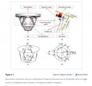
Optimization Design Method of a 6-DOF Micromanipulation Mechanism for Extreme Ultraviolet Projection Lithography Objective Lens.​


National Key Laboratory of Optical Field Manipulation Science and Technology , Chinese Academy of Sciences.

Abstract​


The six-degree-of-freedom (6-DOF) micromotion mechanism is a key component in extreme ultraviolet (EUV) projection lithography objectives to compensate for wavefront aberration and ensure performance stability. It is required to have high precision and high reliability. A 6-DOF mirror micromotion mechanism of an EUV lithography objective lens with Stewart configuration is proposed, and based on the RPY (Roll-Pitch-Yaw) angular rotation method and the second-type Lagrange method, the kinematic and dynamic models of the mechanism are constructed to realize the decoupling of the mechanism’s kinematics and the solution of the driving force. Comparative verification with finite element transient analysis shows that the response value of the dynamic model and the finite element method (FEM) differs by 4.8% in a specific posture. A hybrid optimization method, combining genetic algorithms and particle-swarm optimization (GA-PSO), was proposed to optimize the structural parameters of the initial design of the motion outriggers in a micromotion mechanism. The results demonstrate a 15.1% reduction in maximum driving force, significantly enhancing outrigger driving smoothness.

1721835786554.png

Please, Log in or Register to view URLs content!
 
Top