Chinese semiconductor thread II

interestedseal

Junior Member
Registered Member
Please, Log in or Register to view URLs content!

Interview with AMEC ceo Zhiyao Yin:
1. All components in their tools (etch&thin film) will be indigenized by end of Q3 this year
2. Amec is venturing into e-beam inspection tool
3. 70% tool sale in advanced node
4. optimistic about the whole industry reaching the cutting edge within 3-5 years

I expect the component-level indigenization situation to be similar at Naura and other tool vendors
Here is the interview with AMEC, Piotech, Hwatsing and Skyverse
Please, Log in or Register to view URLs content!
 

Hyper

Junior Member
Registered Member
Please, Log in or Register to view URLs content!

Interview with AMEC ceo Zhiyao Yin:
1. All components in their tools (etch&thin film) will be indigenized by end of Q3 this year
2. Amec is venturing into e-beam inspection tool
3. 70% tool sale in advanced node
4. optimistic about the whole industry reaching the cutting edge within 3-5 years

I expect the component-level indigenization situation to be similar at Naura and other tool vendors
What does point 3 mean.
 

tokenanalyst

Brigadier
Registered Member

Semiconductor front-end measurement equipment supplier Unipro completes a new round of financing of tens of millions of yuan​

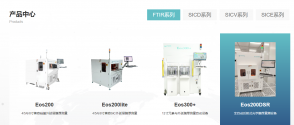
Urepu officially announced that it had recently completed a new round of financing of tens of millions of yuan, led by Clivia Capital, followed by Jingcheng Capital, Zhuoshi Investment, Nantong Haihong Jinsu, etc. This round of financing will be used for the mass production of multiple equipment such as wafer edge detection equipment SICE200, wafer resistivity measurement equipment SICV200, wafer dislocation and micro-pipe detection equipment SICD200, and film thickness measurement equipment Eos200DSR for various semiconductor materials, as well as the research and development of new layout products and the expansion of the team.

Founded in 2021, URP was led by a PhD who has been working in the semiconductor industry for a long time, and co-founded with a senior domestic semiconductor front-end process measurement equipment technology team, committed to creating high-quality semiconductor front-end measurement equipment. In August 2022, URP announced the completion of tens of millions of yuan in Pre-A round of financing, led by Hongzhuo Capital, followed by Yinzhu Capital, Nanjing Xinda Chenghui and Hefei Zhongyu. The funds will be mainly used for the mass production of semiconductor-specific FTIR measurement equipment Eos200/Eos300, Selene series products and the development of new equipment.

In July 2023, Urepu officially announced the completion of nearly 100 million yuan in Series A financing, led by Jishi Pujiang, followed by Hunpu Investment, Galaxy Capital, Zhongnan Venture Capital, Honghu Capital, Hangzhou Menghe, Jingning Lingan and others. The funds will be used for the research and development and mass production of new products. It is reported that Urepu's SICE200 equipment has achieved edge defect detection of compound semiconductors such as silicon carbide, as well as silicon substrates and epitaxial wafers.
1721918174309.png

Please, Log in or Register to view URLs content!
 

tokenanalyst

Brigadier
Registered Member

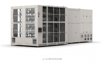
Jingsheng Photonic Cell Equipment of Jingsheng Electronics Co., Ltd. Sets Sail for Overseas Market.​


Recently, the cell equipment independently developed by Zhejiang Jingsheng Photonics Technology Co., Ltd. (hereinafter referred to as "Jingsheng Photonics"), a subsidiary of Jingsheng Electromechanical, was successfully exported to overseas customers. This is not only a solid step taken by the company in its global layout, but also demonstrates the innovative ability and excellent quality of Jingsheng's photovoltaic manufacturing.

With the rapid transformation of the global energy system to low-carbonization, Jingsheng Electromechanical, as a leading enterprise in both technology and scale in the domestic photovoltaic industry, is not afraid of the industrial cycle, and continues to output high-quality photovoltaic equipment in the R&D and manufacturing ends, and continues to promote the upgrading and iteration of equipment technology. As an important part of Jingsheng Electromechanical's layout of the photovoltaic equipment industry, Jingsheng Photonics has always focused on the R&D and manufacturing of high-end equipment in the solar energy field since its establishment last year. It has developed a variety of solar cell process equipment such as tubular PECVD, LPCVD, diffusion and annealing, as well as single-chamber multi-boat ALD and boat dry cleaning. The performance of the equipment has reached or exceeded the same products in the industry.

The products exported overseas by Jingsheng Photonics this time include three latest equipment: PECVD, LPCVD and tubular low-pressure phosphorus diffusion furnace. Among them, the unique filament furnace design of the PECVD equipment makes the efficiency distribution more convergent; the thermal field distribution in the LPCVD equipment cavity is more uniform, and the uniformity of the Poly-Si deposition film thickness exceeds the industry level; the tubular low-pressure phosphorus diffusion furnace innovatively applies flange independent water cooling and other designs to further improve thermal management and airflow control capabilities. The export of these three battery cell equipment overseas will greatly promote the expansion of high-efficiency battery technology and better meet the world's growing demand for clean energy.

1721920343007.png

Please, Log in or Register to view URLs content!
 

kaliko

Just Hatched
Registered Member
Please, Log in or Register to view URLs content!

EDA tools in China used to grow by 20%-40%. Instead, 2023Q4 was weak and 2024Q1 is negative 6.3%. Rest of the world is growing.

It’s not clear whether this is due to a continuing economic slowdown in China, or whether Chinese EDA vendors are developing their own tools, which are not reported in these numbers.

Considering the chinese EDAs are still growing and investing to R&D, the second options is more likely. E.g. Empyrian revenue 213.46M in 2024Q1 is 33% up YoY, with R&D 186.39M.
 
Last edited:

tokenanalyst

Brigadier
Registered Member

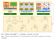
Neutron induced single event effects on near-memory computing architecture AI chips​


Abstract​

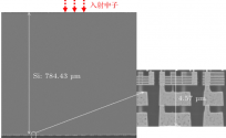
For the near-memory computing architecture AI chip manufactured by using 16 nm FinFET technology, atmospheric neutron single event effect irradiation tests are conducted for the first time in China by using the atmospheric neutron irradiation spectrometer (ANIS) at the China Spallation Neutron Source. During the irradiation, the YOLOV5 algorithm neural network running on the AI chip is used for real-time detection of target objects, including mice, keyboard, and luggage. The purpose of the test is to investigate the new single event effect that may occur on near-memory computing architecture AI chip. Finally, at an accumulated neutron fluence of 1.51×10¹⁰ n·cm–2 (above 1 MeV), a total of 35 soft errors are detected in 5 categories. Particularly noteworthy is the observation of a new finding, where both computing and memory units experience single event effects simultaneously, which is different from the traditional von Neumann architecture chips. Based on the single event effects that occur simultaneously in these two units, combined with Monte Carlo simulation, a preliminary estimation is made of the physical layout distance between the computing unit and the memory unit on the chip. Furthermore, suggestions are proposed to simultaneously reduce the risk of single event effect in multi cells. This study provides valuable reference and insights for further exploring the single event effects in non-traditional von Neumann architecture chips.​

1721940809731.png1721940842102.png

Please, Log in or Register to view URLs content!
 

tokenanalyst

Brigadier
Registered Member

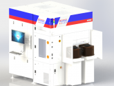
Weichong's first BRAVERY 3000 device was successfully shipped to an important head customer.​


On July 8, 2024, the launch ceremony of the first BRAVERY 3000 equipment of Weichong Semiconductor was officially held. Huang Chongji, founder of Weichong Semiconductor, and co-founders Zhou Puxi and Zhao Weiwei and team members gathered together to witness the exciting moment of the launch of the first BRAVERY 3000 equipment of Weichong. "3, 2, 1, start!" The launch start command was issued, and warm applause and cheers broke out at the scene.

With the launch of the BRAVERY 3000 equipment, the ceremony slowly came to an end. But the story of Weichong Semiconductor has just begun. Weichong heroes will continue to uphold the spirit of innovation, constantly break through themselves, and contribute their own strength to the development of the semiconductor industry. And this exciting moment today will be forever engraved in the memory of Weichong heroes and become the driving force for the team to keep moving forward.

BRAVERY 3000, the core product independently developed by Weichong Semiconductor, is a new type of wafer defect detection equipment with huge market value. It adopts light modulation reflection technology to realize non-contact, non-destructive, online, fast and internal detection of wafers, and accurately diagnose and locate wafer defects. This product is applicable to both patterned and unpatterned wafers, which can fill the gap in the localization of non-contact detection equipment for ion implantation processes in the current domestic market and realize the mass production of ion implantation quality characteristic detection.

1721941831861.png

Please, Log in or Register to view URLs content!
 

tphuang

Lieutenant General
Staff member
Super Moderator
VIP Professional
Registered Member
Please, Log in or Register to view URLs content!

Sanan has 2 new 8-inch SiC production line going into production.

Hunan Sanan's phase 2 going into production with 8-inch SiC. They established full SiC supply chain.

16B total investment here for 360k 6-inch wafers per year and 480k 8-inch

Chongqing fab which is a JV with ST Micro will see its substrate at end of August. Initially, looking for 480k wafers per year of 8-inch here.
 
Top