Chinese semiconductor thread II

tokenanalyst

Brigadier
Registered Member

The Institute of Microelectronics has made progress in the research field of 3D storage for IGZO DRAM back-end integration.​

The rapid development of artificial intelligence has put forward huge demands on hardware resources such as computing and storage, and there is an urgent need to improve the performance and efficiency of memory-level access. At present, the storage system of mainstream computing hardware is composed of on-chip static random access memory (SRAM) and off-chip random dynamic memory (DRAM). Data is transmitted between them through a limited bus, resulting in limited bandwidth, high power consumption and latency. These problems have gradually become a bottleneck for artificial intelligence applications such as big data and high computing power. In addition, the traditional silicon-based six-transistor (6-T) SRAM cell has many limitations in density and energy consumption due to its large feature size and standby leakage problems. At the same time, traditional silicon-based DRAM cells also face problems such as short data retention time and inability to improve storage density through back-end integration. These problems fundamentally limit the power consumption and density of SRAM-DRAM storage systems.

In response to the above problems, the team led by Academician Liu Ming and Researcher Li Ling from the Key Laboratory of Integrated Circuit Manufacturing Technology of the Institute of Microelectronics proposed a new three-dimensional storage structure of IGZO/Si SRAM and IGZO 2T0C DRAM by integrating multi-layer stacked IGZO thin-film transistors (TFTs) with silicon-based circuits, and successfully achieved high-density, low-energy consumption, and high-speed data transmission. In this structure, the IGZO transmission gate is integrated on the front-end silicon-based latch structure, which effectively reduces the occupied space and standby power consumption of SRAM. In addition, based on the vertically stacked three-layer interconnection structure, the lowest delay (<10ns) and lowest energy consumption (2.26fJ) of SRAM-DRAM data transmission are achieved. At the same time, the high data retention characteristics of IGZO 2T0C DRAM enable SRAM to reduce standby power consumption without losing data after a long power outage (>5000s).
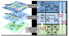
1720468060484.png

The above research results were selected for the 2024 VLSI with the paper titled "First Demonstration of Monolithic Three-dimensional Integration of Ultra-high Density Hybrid IGZO/Si SRAM and IGZO 2T0C DRAM Achieving Record-low Latency (<10ns), Record-low Energy (<10fJ) of Data Transfer and Ultra-long data retention (>5000s)" , and won the Best Demo Paper Award of the conference . This award is only given to two people each year, one each from the process and circuit sub-forums. This work is also the first time that the mainland has won this award. Liu Menggan, Li Zhi and Lu Wendong, doctoral students of the Institute of Microelectronics, are the co-first authors, and Li Ling, a researcher, Yang Guanhua, an associate researcher, and Dou Chunmeng, a researcher of the Institute of Microelectronics, are the corresponding authors.


Please, Log in or Register to view URLs content!
 
Last edited:

tokenanalyst

Brigadier
Registered Member

Jiangsu Xinmeng successfully delivered 12" Cassette-less type tank cleaning equipment.​

As semiconductor technology is changing rapidly, cleaning technology, as a key link to improve product quality and production efficiency, is ushering in a new round of innovation and breakthroughs. Since its establishment, Jiangsu Xinmeng has always insisted on innovation and continued to overcome innovative product technologies. Recently, it has successfully completed the delivery of 12" Cassette-less type tank cleaning equipment , which also marks the further upgrade of its product matrix.

1720468301191.png

· Efficiency and flexibility
The Cassette-less type abandons the limitations of traditional material boxes and supports more direct and efficient loading and unloading methods, including Open Cassette and FOUP. The seamless connection with the OHT system pushes production efficiency to a new level. Its modular design and diverse drying options allow customers to flexibly configure according to specific process requirements, achieving unprecedented cleaning operation efficiency and flexibility.

High cleanliness
Advanced cleaning technologies such as heating, circulation, megasonics and online concentration monitoring are used to ensure that the surface of the silicon wafer reaches an unprecedented high cleanliness standard. It is particularly worth mentioning that the Cassette-less design reduces the contact between the wafer and the additional container, further reducing the risk of contamination. Combined with the environmentally friendly drying method of slow hot water pulling + IR Dry, it not only maintains the extreme cleanliness of the silicon wafer, but also improves the safety of the production process.

Wide applicability
Cassette-less type tank cleaning equipment can easily handle wafers of various sizes, including 4", 6", 8" and 12", covering all areas of the semiconductor industry. From substrate manufacturing to integrated circuits to advanced packaging, it demonstrates its strong applicability.

Customized service
Cassette-less type tank cleaning equipment can not only solve the efficiency and cleanliness problems in the semiconductor cleaning process, but also provide highly customized services. Through a friendly operation interface, excellent material selection, high-quality workmanship and stable mechanical structure, it can well meet the specific needs of different customers .

Please, Log in or Register to view URLs content!
 

tokenanalyst

Brigadier
Registered Member

The Institute of Microelectronics has made progress in the field of high-throughput SRAM in-memory computing processor chips​


At present, the emergence of large-scale AI algorithms such as ChatGPT has put forward higher requirements on the performance of computing devices. Computing in memory (CIM) effectively alleviates the memory wall problem in the traditional von Neumann architecture. Although the memory wall problem cannot be completely solved, the CIM architecture combines storage units and computing circuits through a customized design method, which essentially improves the transmission bandwidth of operands and greatly reduces the transmission cost of this part of data. In recent years, many works on digital CIM architecture processors with high computing energy efficiency have been proposed. These works can achieve high computing energy efficiency when calculating different types of mainstream AI algorithms (such as CNN and Transformer) through customized design of data path control microarchitecture and sparse optimization microarchitecture. However, the computing characteristic of the CIM architecture is that the MAC calculation results are obtained in multiple cycles, and the MAC calculation results cannot be obtained in each cycle after the pipeline is filled like traditional digital circuits. This limits the application scenarios of the CIM architecture to low-power scenarios at the edge, rather than high-performance scenarios. How to solve the shortcomings of insufficient throughput while maintaining the high energy efficiency of the CIM computing architecture is a key issue on the road to the CIM architecture becoming a general architecture in the field of AI computing.
To address this key issue, the team led by Academician Liu Ming and Researcher Zhang Feng from the Institute of Microelectronics of the Chinese Academy of Sciences developed an SRAM in-memory computing processor chip based on Radix16+LUT technology.

At the circuit level, the team used Radix16+LUT technology to reduce the number of INT8*INT8 calculation cycles to 2, achieving 2-cycle calculation at this data precision for the first time (previously the best record was 4 cycles); using LUT technology to minimize the dynamic power consumption overhead of the weight encoding circuit, the circuit calculation power consumption within a single cycle was reduced by 21.7%, ultimately achieving a 1.84-2.44 times reduction in MAC calculation power consumption and a 2-4 times increase in throughput.

At the micro-architecture level, the team proposed a configurable Winograd/Spatial hybrid data path micro-architecture and a pixel/channel hybrid mapping method. A training method is used to determine which level of Winograd algorithm to use at each layer of the algorithm to achieve improved computing throughput.

At the data level, the team fully investigated the representative work of sparse optimization technology in recent years and summarized it by category. Based on these works, a macro-level parallel sparse optimization strategy was proposed. For activation data sparseness, the input data of each macro is grouped together, and the sparse data that can be skipped is selected in a detection-skip manner in groups to achieve sparse activation data optimization. For weight data, the weight data is compressed horizontally by a compact arrangement in the horizontal direction, so as to achieve skipping of the calculation of sparse weight data. The calculated result data is rearranged in the output result register according to the activation data detection index and the weight data index to the data format before the sparse skip operation. In order to reduce the calculation pause caused by sparse optimization, some sparse data is processed in the interval-cycle to achieve latency hiding. This sparse optimization technology solves the problems of limited computational parallelism, special requirements for weight data format, and insufficient versatility of sparse strategies (such as structured sparsity that needs to be retrained) in similar technologies in the past. It is a universal sparse optimization strategy that ultimately helps the processor improve the computing throughput by 3.11 times.

The above design has been verified on the 28nm process, and with the support of the three proposed technologies, it has achieved a peak computing energy efficiency of up to 258.5TOPS/W. Compared with the existing state-of-the-art CIM processor work, its standardized computing throughput has increased by 2.04-3.05 times, and the computing energy efficiency has increased by 2.55-3.45 times.

1720468615279.png 1720468631918.png

Please, Log in or Register to view URLs content!
 

tokenanalyst

Brigadier
Registered Member

ULSI Organic ICs and OLED.​

Fudan University develops semiconductor photoresist to achieve ultra-large-scale integrated organic chip manufacturing​


The Department of Polymer Science of Fudan University has learned that the research team of the school has designed a new type of semiconductor photoresist. Using photolithography technology, they have integrated 27 million organic transistors on a full-frame chip and achieved interconnection, reaching the level of ultra-large-scale integration (ULSI).
On July 4, 2024, this achievement was published in Nature Nanotechnology under the title "High-performance large-scale integrated organic phototransistors based on photovoltaic nanounits".
Chip integration can be divided into small-scale integration (SSI), medium-scale integration (MSI), large-scale integration (LSI), very large-scale integration (VLSI) and ultra-large-scale integration (ULSI). Previously, the manufacturing methods of organic chips mainly included screen printing, inkjet printing, vacuum evaporation, photolithography, etc., and the integration level could usually only reach the large-scale integration (LSI) level.
Photoresist, also known as photoresist, plays a key role in chip manufacturing. It can transfer the required fine patterns from the mask to the substrate to be processed through processes such as exposure and development. It is a basic material for photolithography process.
The Fudan team designed a new functional photoresist composed of a photoinitiator, a cross-linking monomer, and a conductive polymer. After photocrosslinking, a nanoscale interpenetrating network structure is formed, which has good semiconductor performance, photolithography processing performance, and process stability. This photoresist can not only realize the reliable manufacture of sub-micron feature size patterns, but the pattern itself is a semiconductor, thus simplifying the chip manufacturing process.
The organic transistor interconnect array manufactured by photolithography contains 4500×6000 pixels, with an integration density of 3.1×10⁶ units per square centimeter, that is, 27 million devices are integrated on a full-frame chip, achieving ultra-large-scale integration (ULSI). Its photosensitivity reaches 6.8×10⁶ amperes per watt. The high-density array can be transferred to a flexible substrate, realizing bionic retinal applications.

Please, Log in or Register to view URLs content!
 

ansy1968

Brigadier
Registered Member
asml has now released the NXT:1980Fi:
Please, Log in or Register to view URLs content!
I don't know if that's a rebranded NXT 2000i, ban under the new restrictions, if it is then its too late, the current SSA800A iteration is comparable and a newer DUVI 2 (22nm SSA900 comparable to NXT 2050i) will be introduced next year, so the window is shrinking fast and the former ASML CEO knew it.
 

tokenanalyst

Brigadier
Registered Member

Dinglong shares: polysilicon polishing liquid and silicon nitride polishing liquid products received tens of millions of yuan in batches of orders​

Dinglong Co., Ltd. issued an announcement stating that the company's holding subsidiary, Wuhan Dingze New Materials Technology Co., Ltd. (hereinafter referred to as "Dingze New Materials"), located in the Xiantao Park, has an annual production capacity of 10,000 tons of CMP polishing liquid (Phase I) and an annual production capacity of 10,000 tons of CMP polishing liquid for supporting nano-abrasive particles. The production line was completed and put into trial production in November 2023. After the company's efficient trial production, process integration, and close factory inspections and production line verification with customers, it now has the ability to mass-produce in large quantities and on a stable scale.
Recently, after a strict product quality review by a mainstream domestic wafer factory customer, the polysilicon (Poly-Si) polishing liquid and silicon nitride (SiN) polishing liquid products produced by Xiantao Park (with Xiantao's own abrasive particles) have obtained a batch order of tens of millions of yuan for the first time. In addition, the company's above-mentioned polishing liquid products are being verified simultaneously by other mainstream domestic wafer factory customers, and are currently progressing smoothly.
This is an important progress made by Dinglong Co., Ltd. in improving and expanding the company's CMP polishing liquid production capacity layout and promoting rapid growth of this business following the continuous increase in sales of CMP polishing liquid products of the company's Wuhan headquarters at the client end.​
 

broadsword

Brigadier
Huawei Reportedly to Launch Kirin 9100 with Superior Performance to Snapdragon 8 Gen 2
2024-07-08 Consumer Electronics / Semiconductors editor

According to a report from Wccftech, Huawei’s Kirin 9100 processor is scheduled to be unveiled later this year, rumored to be manufactured using SMIC’s 5nm process. Its performance is reported to surpass that of the Qualcomm Snapdragon 8 Gen 2, and it will be featured in the entire Mate 70 series of smartphones.

The same report cited industry sources, suggesting that SMIC has successfully produced 5nm chips using DUV lithography instead of EUV, which is typically required for 5nm production. The high cost and low yield of DUV make it a challenging feat for most manufacturers. Fortunately, this breakthrough could help Huawei narrow the performance gap in its processors.

Reportedly, the Kirin 9100 is rumored to outperform the Snapdragon 8 Gen 2 overall and offer interface smoothness comparable to the Snapdragon 8 Gen 3. Huawei’s software optimization is anticipated to contribute significantly, as the company plans to launch HarmonyOS NEXT this year, completely moving away from the Google Android framework.

The report notd that switching to HarmonyOS NEXT has advantages, including memory usage that is three times more efficient than Android, and stringent resource consumption management. The new system can also be installed on older Huawei smartphones with previous-generation Kirin processors. Thanks to the 5nm process, the Kirin 9100 will also have improved energy efficiency. However, the actual performance will need to be verified once Huawei releases more detailed information.
 
Top