Chinese semiconductor thread II

tphuang

Lieutenant General
Staff member
Super Moderator
VIP Professional
Registered Member
couple of interesting weibo post from the guy that broke the huawei 5g news
自研小芯片+1,今年核心线小芯片已落地两颗,好好好!
This likely talks about Xiaomi, they have 2 SoC designed that will land this year

虽然年底新旗舰落地了单框架自研OS+新一代自研5G SOC+50Mp国产超大底CIS,但还有一个更加重量级的产品,工业难度让友商望而却步,现阶段良率极低,但计划是准备量产的,攻坚中
this likely talks about Huawei, the first phone is M70 confirmed to be using new self designed OS, new generation 5G SoC (Kirin 9100?) and 50 Mp domestic flagship CIS (OV50K?)

But apparently they have an even higher end phone in product lineup whose engineering difficulty has deterred competition. So far, yield is still quite low but they still plan to mass produce. This is likely the 3-fold phone, which can be unfolded to size of a pad to be used for work purpose. Exciting times.
 

JPaladin32

Just Hatched
Registered Member
couple of interesting weibo post from the guy that broke the huawei 5g news

This likely talks about Xiaomi, they have 2 SoC designed that will land this year


this likely talks about Huawei, the first phone is M70 confirmed to be using new self designed OS, new generation 5G SoC (Kirin 9100?) and 50 Mp domestic flagship CIS (OV50K?)

But apparently they have an even higher end phone in product lineup whose engineering difficulty has deterred competition. So far, yield is still quite low but they still plan to mass produce. This is likely the 3-fold phone, which can be unfolded to size of a pad to be used for work purpose. Exciting times.
If you think about it, normal foldables have an outer display and an inner larger one. When you unfold you won't be using the outside screen, but with 3-fold you are using all available screen real estate when unfolded, so 3-fold kind of makes sense without adding extra screen hardware.
 

tokenanalyst

Brigadier
Registered Member

Leuven Instruments' patent for "A method for repairing lattice defects on the surface of epitaxial wafers" was published​


Tianyancha shows that Jiangsu Leuven Instrument Co., Ltd.’s patent for “A method for repairing lattice defects on the surface of wafer epitaxial wafers” has been announced. The application publication date is June 28, 2024, and the application publication number is CN118263091A.

The present invention relates to the field of semiconductor chip production, and specifically to a method for repairing lattice defects on the surface of a wafer epitaxial wafer. The present invention provides a method for repairing lattice defects on the surface of a wafer epitaxial wafer. The method provided by the present invention uses an oxidizing gas such as N2O or O2 plasma to treat the surface of the wafer epitaxial wafer to form a uniform oxide layer; uses a chlorine-based gas such as BCl3 plasma to treat the surface of the oxide layer to uniformly remove the oxide surface layer; uses a mixed gas of chlorine-based gas and fluorine-based gas or chlorine-based gas plasma to etch the surface of the material, which can effectively optimize the lattice defects generated in the epitaxial growth process of the surface layer of the wafer epitaxial wafer or the etching defects and damage caused by oxidation spots, thereby obtaining a wafer epitaxial wafer with high uniformity and consistency; compared with the prior art, the present invention has a better effect of removing the lattice defect layer on the surface of the wafer epitaxial wafer.

Please, Log in or Register to view URLs content!
 

tokenanalyst

Brigadier
Registered Member

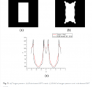
Fast and high-fidelity EUV curvilinear mask optimization by distance-versus-angle signature​

Abstract​


Curvilinear mask has received much attention in recent years due to its ability to obtain better image quality in advanced nodes. A common method for optimizing curvilinear mask in optical proximity correction (OPC) flow is moving control points on the edge directly (MCED-based OPC), but it requires storing mass data. This paper uses distance-versus-angle signature (DVAS), a one-dimensional function, to represent a two-dimensional boundary of mask. To the best of our knowledge, DVAS and its second derivative are applied for the first time to reduce the design data storage space and guide the direction of optimization in EUV lithography systems. Compared with storing the change distances of the control point in both horizontal and vertical directions, directly storing the amplitude change of the DVAS can effectively reduce the storage space consumption. Simulation results demonstrate that unlike the MCED-based OPC method, the DVAS-based OPC method using second derivative achieves a lower pattern error and requires less time while reducing the storage space.

1720466273411.png
Please, Log in or Register to view URLs content!
 

tokenanalyst

Brigadier
Registered Member

Vacuum cleaning of amorphous carbon using hydrogen plasma for EUV lithography​


School of Microelectronics, Shanghai University
Materials Genome Institute, Shanghai University
School of Mechatronic Engineering and Automation, Shanghai University

Abstract​

EUV lithography has a promising application, but carbon contamination limits its efficiency and service lifetime. The key issue is how to remove carbon contaminations efficiently and non-destructively on EUV optics. Plasma cleaning technology has been proven to clean carbon effectively. However, the surface reaction mechanism underlying plasma cleaning of carbon contamination remains incompletely understood. To analyze the mechanism of carbon removal via plasma treatment, we first experimentally investigated the effects of different macro conditions (RF power and pressure) on plasma cleaning of carbon contamination. Subsequently, the chemical properties, along with the surface roughness and morphology of the substrates were analyzed, utilizing Raman spectroscopy, XPS, contact angle measurements and AFM. The effectiveness of plasma in removing amorphous carbon, restoring surface character, and inducing changes in surface morphology and roughness was revealed. These findings provide important clues for realizing in-situ non-destructive cleaning of EUV optics.

Please, Log in or Register to view URLs content!
 
Top