Chinese semiconductor thread II

tokenanalyst

Brigadier
Registered Member

The Institute of Microelectronics has made important progress in studying the threshold voltage instability mechanism of GaN-based MIS-HEMT devices​

Source: Huang Sen, High Frequency and High Voltage Center Release time: 2024-06-11
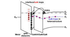
Recently, the GaN power electronic device research and development team of the High Frequency and High Voltage Center of the Institute of Microelectronics, together with the Hong Kong University of Science and Technology, Peking University and Xidian University, published a review article titled "Threshold voltage instability in III-nitride heterostructure metal-insulator-semiconductor high-electron-mobility transistors : Characterization and interface engineering " in Applied Physics Reviews, an international authoritative journal in the field of applied physics. This work uses advanced interface state and body defect characterization methods to reveal the physical mechanism of threshold voltage instability of GaN-based heterojunction power devices. Aiming at the dynamic instability problem of GaN-based MIS-HEMT based on two common gate/passivation dielectrics, Al2O3 and SiNx , an innovative process that effectively suppresses surface interface states and dielectric defect states has been developed, which has promoted the development of the next generation of high-reliability GaN-based insulated gate power devices.
1718137396092.png

Compared with traditional semiconductor materials such as Si, GaN-based MIS/MOS-HEMT power devices based on metal-insulator-semiconductor (MIS) or metal-oxide-semiconductor (MOS) gate structures can operate at higher voltages, higher frequencies and higher temperatures, and have broad application prospects in high-efficiency power conversion, RF power amplifiers and extreme environment electronics. However, due to factors such as natural oxidation and process contamination, the surface of GaN materials easily loses the step flow morphology of the original fresh surface, thereby inducing a high-density surface state on GaN, leading to reliability problems such as current collapse of GaN-based power devices. On the other hand, in MIS/MOS structure power devices, there are also a large number of body defects in the gate dielectric and AlGaN/GaN heterostructures. Once these defect states, especially the gate dielectric defect states, are filled, it is difficult to release, resulting in more serious threshold voltage instability problems.

Based on first principles and surface physical and chemical analysis, the research team found that the shallow energy level interface states of GaN mainly originate from the strong interaction between Ga dangling bonds and atoms near its interface (ACS AMI, 10, 21721, 2018 & 13, 7725, 2021), while the deep energy level interface states are mainly related to the amorphous Ga2O chemical state on the surface , and its cracking temperature is above 450°C. Based on this , the research team innovatively proposed the "high-temperature remote plasma pretreatment (RPP)" method, which achieved the stable reproduction of atomic steps on the GaN surface with different surface conditions. The new "high-temperature RPP" method reduced the deep energy level interface state density of oxide/GaN represented by Al2O3 and nitride/GaN represented by SiNx by at least one order of magnitude. Among them, the SiNx / GaN interface state density has a minimum value of 1.5×10¹⁰eV-1cm-2 in the wide energy level range of 30meV-0.9eV , which is close to the optimal level of Si-based MOS devices. In order to characterize the gate interface state/body defects of GaN-based MIS-HEMT devices, the research team innovatively developed multiple modes of deep energy level transient spectroscopy (DLTS) rapid characterization methods such as "isothermal capture" and "constant capacitance", realizing the metal/insulator/AlGaN/GaN "multi-heterogeneous interface" The effective separation of body defects and interface states in heterojunction power devices reveals the correlation mechanism between dynamic on-resistance degradation, threshold voltage instability and interface/dielectric process of GaN-based MIS-HEMT power devices, providing important physical feedback for the reinforcement of the next generation of high-reliability GaN-based insulated gate power devices.

Please, Log in or Register to view URLs content!
 

PikeCowboy

Junior Member
For Apple, I haven't checked all the details, but the logic should be sound.
1: Due to the lithography limitation in China, it looks like Apple would always have better logic and memory chips. With AI features moving to edge devices, Apple's enhanced computing power(M4 chip is a beast) becomes more appealing. Satcom/Photography noncore functions.
2: IOS is a much more mature and huge ecosystem, I doubt foreign App/Game developers would migrate their products to the HarmonyOS, I guess there are "emulators" that can be used to run Android apps in HarmonyOS. Lack of App/Game support is a no-go for lots of people. Unless Huawei is able to vastly ramp up advanced node production, then flooding the market with cheap, high-quality devices, without much higher market shares, very hard for HarmonyOS to compete with IOS.
3: Global after-sale support and brand awareness, I doubt people can get after-sale service outside of China.
4: I saw some people posting on social media, with multiple discounts, Apple iPhone 15 Pro 256G is selling for around 6300RMB in China, the same price level as Mate 60 Pro, Unless people want to support Huawei, there are no compelling reasons to buy Huawei over Apple when they are on the same price level.

If you are a light phone user, just check social media posts or watch videos on TikTok, any phone would do the job, won't notice any difference.

For Nivida,
1: H20 and 910B prices similarly in China, 910B maybe slightly faster, but H20 is manufactured by TSMC with better processing nodes, H20 should be more mature and stable.
2: Nivida's CUDA ecosystem is so entrenched, without the geopolitical risk factors, so much easier to build your system with CUDA. Recently some news mentioned some big tech companies are planning to build data centers in the West (or rent AI chips) to avoid the sanctions in order to buy Nivida's chips.
yeah but if you use cuda youre locking your self into a dead end...
 

tokenanalyst

Brigadier
Registered Member

Gate All Around Complementary FET Based 6T SRAM Path-Finding​

Chinese Academy of Science Institute of Microelectronics Beijing, China
School of Integrated Circuits University of Chinese Academy of Sciences Beijing, China

Abstract:​

Vertical Gate All Around Nanowire Complementary FET based logic circuits offer an alternative way for higher cell density without aggressive gate length scaling. In this study, we develop a device to circuit design-technology co-optimization (DTCO) flow that incorporates Virtual Fab Semiconductor Process Modeling and physics-based TCAD simulations. We compare VGAA Complementary FET (CFET) based 6T SRAM with its counterparts by conventional planar CMOS, sequential/monolithic 3DIC CFETs with lateral transistors, accounting for the parasitics from virtual fab modeling. Our results show that VGAA CFETs offer better control over the channel and reduce parasitic capacitances and resistances compared to the counterpart technology options.​

Please, Log in or Register to view URLs content!
 

dingyibvs

Senior Member
Photons are way too energetic. Resist outgassing is a huge problem. Photomask may not survive the damage. All in all lithography will run out of steam. ASML will continue to fine tune and upgrade the machines but the idea of a big technological jump is impossible. Samsung is planning 3D DRAM starting production in early 2030s. Embedded systems will introduce MRAM. I doubt leading edge logic really wants to beat such high costs of lithography based scaling. They will focus on cfet and 2D materials.
Just curious, but are there any potential disruptive techs in other chipmaking steps similar to FEL/synchrotron based light source in lithography?
 

Hyper

Junior Member
Registered Member
Just curious, but are there any potential disruptive techs in other chipmaking steps similar to FEL/synchrotron based light source in lithography?
Don't need any disruption. Current process need incremental advances for future nodes. But if you ask them yes selective deposition and etch and also dry resist are advances for scaling. Subtractive etch is also important for future interconnects.
 

tonyget

Senior Member
Registered Member
Please, Log in or Register to view URLs content!

US Weighs More Limits on China’s Access to Chips Needed for AI​

  • Restrictions would target novel ‘gate all-around’ technology
  • US officials are in early talks on high-bandwidth memory curbs
The Biden administration is considering further restrictions on China’s access to chip technology used for artificial intelligence, targeting new hardware that’s only now making its way into the market, people familiar with the matter said.

The measures being discussed would limit China’s ability to use a cutting-edge chip architecture known as gate all-around, or GAA, according to the people, who spoke on condition of anonymity because the deliberations are private. GAA promises to make semiconductors more powerful and is currently being introduced by chipmakers.

It’s unclear when officials will make a final decision, the people said, emphasizing that they’re still determining the scope of a potential rule. The US goal is to make it harder for China to assemble the sophisticated computing systems needed to build and operate AI models, they said — and to cordon off still-nascent technology before it’s commercialized.

Companies such as Nvidia Corp., Intel Corp. and Advanced Micro Devices Inc. — along with manufacturing partners Taiwan Semiconductor Manufacturing Co. and Samsung Electronics Co. — are looking to start mass-producing semiconductors with the GAA design within the next year.

The US has already imposed numerous restrictions on the sale of advanced semiconductors and chipmaking tools to China. Commerce Secretary Gina Raimondo has repeatedly said the US will add to those measures as needed to keep the most advanced AI technology out of Beijing’s hands, over fears that it could give an edge to China’s military.

Still, the Biden administration is running against the clock on issuing additional regulations before the November presidential election and juggling which technologies to prioritize.

A spokesperson for the Commerce Department’s Bureau of Industry and Security, which oversees export controls, declined to comment. A representative of the National Security Council did not respond to a request for comment.

BIS recently sent a draft GAA rule to what’s known as a technical advisory committee, some of the people said. The panel is composed of industry experts and offers advice on specific technical parameters — a final step in the regulatory process.

But the rule is not yet finalized, according to the people, after industry officials criticized the first version as overly broad. It’s unclear whether the ban would restrict China’s ability to develop its own GAA chips or go further and seek to block overseas companies — particularly US chipmakers — from selling their products to Chinese electronics manufacturers.

One person familiar with the matter said the measures wouldn’t go as far as an outright ban on GAA chip exports, but instead focus on the technology needed to make them.
 

paiemon

Junior Member
Registered Member
yeah but if you use cuda youre locking your self into a dead end...
Its going to take a while to move off Nvidia, it is a huge sunk cost and as long as they can keep using it, they will squeeze whatever they can out of what they have. Switching is not a simple porting over exercise from CUDA to the Huawei framework, a complete code base re-design and overhaul would be needed. It goes far beyond refactoring because your code logic, systems design, architecture, basically everything was built with the assumption of using CUDA libraries, extensions, etc. Even if Huawei provided an easy toolkit for porting such as an interpreter to make it more adaptable, unless their architecture is similar to CUDA or they provide cross-compatibility your code would not work properly without big changes or would have large quality issues. We are talking millions of lines of code that would need to examined, documented, re-designed and re-implemented which is a huge sustaining engineering effort. As an example, a game that runs on PS4/PS5 versus one that runs on PC would need two different codebases because the Playstation hardware architecture requires far more SW optimization than their PC counterparts. Switching to a domestic system would have to be a gradual parallel effort because you simply cannot afford to drop everything cold turkey without losing months of work at a minimum.
 

tokenanalyst

Brigadier
Registered Member

Suzhou Xinrui's first Aviator 12-inch advanced packaging temporary bonding (TB) equipment was successfully launched.​

On June 11, 2024, CoreRay Technology's first Aviator 12-inch advanced packaging temporary bonding (TB) equipment was officially delivered to the client.

R&D and manufacturing team

The equipment was independently developed by Suzhou Xinrui Technology. It is completely independent of imports and its main performance indicators are comparable to similar foreign products, adding a new force to domestic substitution.

Subsequently, Suzhou Xinrui Technology will enter a more intense equipment debugging and production preparation phase, and will make every effort to promote the project to achieve production capacity targets as scheduled.

1718166579396.png


Delivery

In the golden age of the rise of China's semiconductor industry, Suzhou Coreray Technology will continue to take technological innovation as the primary driving force, helping the Suzhou Industrial Park to consolidate the foundation for industrial development and contribute to China's semiconductor industry.

Aviator series temporary bonding equipment ABT-12 inch

1718166610772.png

Specifications:


Wafer size: 300mm(12")

Bonding pressure: ≤ 60kN

Bonding temperature: ≤ 350°C

Chamber vacuum: 10-2mbar

Bond offset: ≤ 0.1mm

Product Introduction:

ABT-12 is a fully automatic temporary bonding equipment, equipped with glue spreading and wafer transfer system, mainly used in advanced packaging, such as WLCSP, FOWLP, 2.5D, 3D, etc.

Product advantages:

We can provide comprehensive bonding and debonding solutions for advanced packaging, providing customers with one-stop service, and our prices are very competitive compared to similar foreign equipment.

Please, Log in or Register to view URLs content!
 
Top