Chinese semiconductor thread II

tokenanalyst

Brigadier
Registered Member
Actually, from the comment area on that original bilibili video(which has been deleted now). Someone mentioned that the single expose area of ASML is about 6 times of that kirin9010 die area,and one expose only requires one alignment mark,so six dies only require one alignment mark. So it is possible that the die he is got,just happen to be the one without alignment mark,and the video creator agree with this speculation.
I have my doubts, wafers are cut with a lot of precision, especially that ones with such high cost dies.
Also a bad position of the mark would mean some miss alignment problem that would render the entire wafer bad.
Maybe could be that the changed the overlay, ASML scanners allow ways for user overlay methods.
 

tokenanalyst

Brigadier
Registered Member

Beijing Integrated Circuit Industry-Education Integration Base will be put into use in September next year​


According to Beijing Yizhuang news, the underground structure of the Beijing Integrated Circuit Industry-Education Integration Base project has recently broken through the "zero point", which means that the project has fully entered a new stage of ground steel structure construction. The total construction area of the project is 105,524 square meters, and four teaching and research buildings with 11 floors above ground and 3 floors underground will be built. After the project is completed, it can accommodate 2,000 people for on-campus training at the same time.

According to reports, the project will start in June 2023 and is expected to be put into use in September 2025. By creating an "efficient, open, healthy and shared" park environment, it will promote production through teaching and assist teaching through production.
In order to strengthen the effective supply of integrated circuit talents and promote the high-quality development of the integrated circuit industry, the Beijing Integrated Circuit Industry-Education Consortium was established in Beijing Economic and Technological Development Zone in June 2023. In September 2023, the Beijing Integrated Circuit Industry-Education Consortium was shortlisted for the first batch of 28 national-level municipal industry-education consortia announced by the Ministry of Education.

According to a report by Xinhua News Agency in March this year, the Beijing Integrated Circuit Industry-Education Consortium is a government-school-enterprise consortium established based on the Beijing Economic and Technological Development Zone and adopting the operating model of "government-led, school-based, and enterprise-coordinated". The Beijing Yizhuang Management Committee plays a leading role in the government, and Beijing Electronic Science and Technology Vocational College serves as the secretary-general unit, in conjunction with more than 30 units including Beijing University of Technology, North China University of Technology, Beijing Integrated Circuit Excellent Engineer Innovation Institute, and the North Integrated Circuit Technology Innovation Center, SMIC, and North China Huachuang.

Please, Log in or Register to view URLs content!
 

LuzinskiJ

Junior Member
Registered Member
Not sure if it applies to this article in particular, but my understanding was the US lawmakers were attempting to restrict commercial activity between US and/or Chinese implementations of the architecture. That is to say, import/export controls on the hardware, designs, and so on.

Which is still dumb, but not impossible.
Or simply pass laws to sanction any Chinese companies working on the design, fabrication or manufacturing based on RISC-V architecture. Sanction has become a go-to instrument for the US law makers since it is easy to do, so I think it will be their approach this time around as well.
 

tokenanalyst

Brigadier
Registered Member
Not sure if it applies to this article in particular, but my understanding was the US lawmakers were attempting to restrict commercial activity between US and/or Chinese implementations of the architecture. That is to say, import/export controls on the hardware, designs, and so on.

Which is still dumb, but not impossible.

Or simply pass laws to sanction any Chinese companies working on the design, fabrication or manufacturing based on RISC-V architecture. Sanction has become a go-to instrument for the US law makers since it is easy to do, so I think it will be their approach this time around as well.

An ISA is just a set of instructions to create processors that run RISC-V compiled software, yes the US stooges can put export controls on US commercial Emulators and designs, good luck putting controls on things that are public in the web, but there is nothing that would stop a Chinese company from creating their own designs and RISC-V ecosystem. And ISA is just a BOOK. A PDF file. That only thing that stooges will achieve is to US companies pull out of the standard and Chinese companies becoming the dominant player.

For god sake, China have companies that make X86, MIPS and even RDNA processors. Huawei has a permanent ARM license, ARM is not constantly supplying Huawei with updates on tools and designs, Huawei has to create most of their ARM tools and design from the ground up .

Here this is what you need:
Please, Log in or Register to view URLs content!

Chinese company that created their own ecosystem basically from zero, one of the first companies that joined the standard.
Please, Log in or Register to view URLs content!
 

tokenanalyst

Brigadier
Registered Member

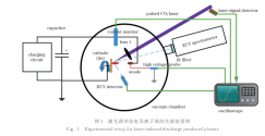
Research on laser-induced discharge plasma extreme ultraviolet light source​


Guangdong Greater Bay Area Aerospace Information Research Institute
Wuhan National Optoelectronics Research Center
University of Chinese Academy of Sciences
Russia Research Center Kurchatov Institute

Abstract​

Extreme ultraviolet light sources have important applications in mask inspection, microscopy imaging and spectral measurement in semiconductor manufacturing. Laser-induced discharge plasma is one of the important technical means to generate extreme ultraviolet light sources. An experimental device was built to generate tin plasma by carbon dioxide laser-induced discharge. The generated extreme ultraviolet spectrum was collected and detected, combined with radiation magnetohydrodynamics. Chemical simulations were performed to analyze the radiation characteristics of extreme ultraviolet. The experiment compared the differences in the extreme ultraviolet radiation characteristics of laser plasma and discharge plasma, and found that the discharge voltage has an important influence on the in-band radiation intensity of laser-induced discharge plasma extreme ultraviolet light. The simulation found that when the voltage is 15kV, the total energy of extreme ultraviolet radiation reaches 65.0mJ. The conversion efficiency reaches 0.23%, and the spectral purity reaches 1.69%.​

1717692020855.png

Please, Log in or Register to view URLs content!
 

european_guy

Junior Member
Registered Member

Huawei says its AI chip better than Nvidia’s A100 amid China’s self-reliance drive​


Please, Log in or Register to view URLs content!


A Huawei Technologies executive said the company’s latest artificial intelligence (AI) chip is on par with, if not better than
Please, Log in or Register to view URLs content!

Huawei’s Ascend 910B AI chip has been found in some tests to deliver 80 per cent of the efficiency of an Nvidia A100 when training large language models, but “in some other tests, Ascend chips can beat the A100 by 20 per cent”, said Wang Tao, chief operating officer of Huawei Ascend and Kunpeng ecosystem, on the sidelines of the
Please, Log in or Register to view URLs content!
on Thursday.


The NVIDIA A100 chip was presented in 2020
Please, Log in or Register to view URLs content!
and is still the workhorse for AI training in data centers around the world.
 

Wrought

Junior Member
Registered Member
An ISA is just a set of instructions to create processors that run RISC-V compiled software, yes the US stooges can put export controls on US commercial Emulators and designs, good luck putting controls on things that are public in the web, but there is nothing that would stop a Chinese company from creating their own designs and RISC-V ecosystem. And ISA is just a BOOK. A PDF file. That only thing that stooges will achieve is to US companies pull out of the standard and Chinese companies becoming the dominant player.

For god sake, China have companies that make X86, MIPS and even RDNA processors. Huawei has a permanent ARM license, ARM is not constantly supplying Huawei with updates on tools and designs, Huawei has to create most of their ARM tools and design from the ground up .

Here this is what you need:
Please, Log in or Register to view URLs content!

Chinese company that created their own ecosystem basically from zero, one of the first companies that joined the standard.
Please, Log in or Register to view URLs content!

I know, that's why I said it was dumb. But there is nothing impossible about doing dumb stuff, and we've certainly seen them do it in the past.
 

tokenanalyst

Brigadier
Registered Member
Semiconductor Diamond photolithography Etching.​

High-precision and high-speed etching of diamond surfaces using Fe–Ni alloy catalyzed H–O plasma etching​

Abstract​

Power devices with low losses are essential for achieving high-efficiency, low-cost, and miniaturized inverters and advance electronic technologies. Recently, diamond-based p-type groove semiconductor field-effect transistors have emerged as a hot research topic. Conventional method of fabricating surface grooves using inductively coupled plasma etching is costly and relatively slow. Here, we realized a novel diamond machining method using Fe–Ni alloy catalyzed H–O microwave plasma etching that can achieve high-rate and high-precision etching of diamond surfaces. Two major factors affecting the etching rate and pattern accuracy, wettability of diamond and carbon solubility with liquid metal, were identified. Oxygen added in H2 plasma allows the wetting increase, resulting in an improvement in uniformity of the etch area, while keeping the etch rate as high as 3 μm/min. The developed approached is promising for low-cost diamond patterning in electronic devices fabrication processes.

1717702592734.png

Material and methods​

The experiment consisted of three steps: photolithography, coating, and etching. The single-crystal diamond plates (Hubei Carbon Six Technology Co., Ltd.) grown by chemical vapor deposition (CVD) were used as the substrates. The plates had a thickness of 0.5 mm, a size of 5 × 5 mm, and (100) crystal planes on all six sides. A home-made microwave plasma chemical vapor deposition (MPCVD) system (HITLH-2450 M) for diamond growth was used for the etching experiments.


Please, Log in or Register to view URLs content!
 

tokenanalyst

Brigadier
Registered Member
The HomeMade MPCVD tool.
Semiconductor Diamond photolithography Etching.​

High-precision and high-speed etching of diamond surfaces using Fe–Ni alloy catalyzed H–O plasma etching​

Abstract​

Power devices with low losses are essential for achieving high-efficiency, low-cost, and miniaturized inverters and advance electronic technologies. Recently, diamond-based p-type groove semiconductor field-effect transistors have emerged as a hot research topic. Conventional method of fabricating surface grooves using inductively coupled plasma etching is costly and relatively slow. Here, we realized a novel diamond machining method using Fe–Ni alloy catalyzed H–O microwave plasma etching that can achieve high-rate and high-precision etching of diamond surfaces. Two major factors affecting the etching rate and pattern accuracy, wettability of diamond and carbon solubility with liquid metal, were identified. Oxygen added in H2 plasma allows the wetting increase, resulting in an improvement in uniformity of the etch area, while keeping the etch rate as high as 3 μm/min. The developed approached is promising for low-cost diamond patterning in electronic devices fabrication processes.

View attachment 130714

Material and methods​

The experiment consisted of three steps: photolithography, coating, and etching. The single-crystal diamond plates (Hubei Carbon Six Technology Co., Ltd.) grown by chemical vapor deposition (CVD) were used as the substrates. The plates had a thickness of 0.5 mm, a size of 5 × 5 mm, and (100) crystal planes on all six sides. A home-made microwave plasma chemical vapor deposition (MPCVD) system (HITLH-2450 M) for diamond growth was used for the etching experiments.


Please, Log in or Register to view URLs content!

Vapor phase nucleation and sedimentation of dispersed nanodiamonds by MPCVD.​

Abstract​

Microwave plasma assisted chemical vapor deposition (MPCVD) is a technique for preparing high-quality diamonds. However, the low yield and easy bonding between particles are drawbacks in the preparation of nanodiamond (ND). These issues are mainly caused by the adverse phenomena such as substrate nucleation and the continuous growth of particles. To inhibit these phenomena, diamond vapor phase nucleation (VPN) is realized by adjusting the spatial distribution of the carbon and hydrogen groups in plasma. In this environment, NDs nucleate, grow and fall on the disk. As such, dispersed nanodiamonds are obtained and the yield limit of MPCVD prepared NDs is broken. Further, we analyze and improve the VPN growth mechanism. This study presents a new mode of using MPCVD, which can be used to grow dispersed NDs. The development and improvement of this method is expected to provide higher quality NDs for drug transportation, biological imaging, and quantum light sources.

Experimental section​

The home-made MPCVD diamond growth system (HITLH-2450 M) [19] developed by the author's laboratory was used to prepare NDs. The microwave at 2.45GHz frequency is generated by the microwave generator and transmitted in TE mode through the waveguide. At the converter, it becomes TM mode and enters the stainless steel resonant chamber. Based on the shielding effect of metal on microwave, molybdenum cylinder (MoC, φ = 8 mm, XMo = 5 mm.​

Please, Log in or Register to view URLs content!
 
Top