Chinese semiconductor thread II

AndrewS

Brigadier
Registered Member
Please, Log in or Register to view URLs content!

Beijing SMIC non-US line is operational at 28nm 2nd half of the year. No Applied, No Lam and No KLA.

Some comments on the article.

1. There's no mention of SMEE or DUV lithography machines in this de-Americanised fab, which is a very curious omission

2. "It is now capable of producing chips as advanced as 28-nanometer circuits at this line, and recent output volume there is already beyond the pilot production level, a person familiar with the matter said"
 

sunnymaxi

Major
Registered Member
Some comments on the article.

1. There's no mention of SMEE or DUV lithography machines in this de-Americanised fab, which is a very curious omission

2. "It is now capable of producing chips as advanced as 28-nanometer circuits at this line, and recent output volume there is already beyond the pilot production level, a person familiar with the matter said"
WSJ is outdated with a margin ..

we already have 14nm De-Americanized line.. 28nm complete domestic line has been established last year..
 

measuredingabens

Junior Member
Registered Member
Some comments on the article.

1. There's no mention of SMEE or DUV lithography machines in this de-Americanised fab, which is a very curious omission

2. "It is now capable of producing chips as advanced as 28-nanometer circuits at this line, and recent output volume there is already beyond the pilot production level, a person familiar with the matter said"
Given how closely guarded DUVi and EUV is, I'd be very surprised if they outright admitted to using SMEE's scanners. Besides, fully domestic 28nm was already in production last year, this year is 14nm and maybe 7nm depending on their pace. On that note, I do wonder if 3nm will be the first node where Huawei and SMIC go fully domestic from the get go, as they certainly aren't getting any new western tools and Chinese toolmakers are rapidly catching up to the global leading edge.
 

sunnymaxi

Major
Registered Member
Given how closely guarded DUVi and EUV is, I'd be very surprised if they outright admitted to using SMEE's scanners. Besides, fully domestic 28nm was already in production last year, this year is 14nm and maybe 7nm depending on their pace. On that note, I do wonder if 3nm will be the first node where Huawei and SMIC go fully domestic from the get go, as they certainly aren't getting any new western tools and Chinese toolmakers are rapidly catching up to the global leading edge.
SMIC Finfet capacity is going to be double.. 70k wpm.. outside Lithography rest majority of tools are from Chinese firms..

since October, 2022.. US tools makers didn't supply any type of Finfet capable tool to China.. not even service/repair and maintenance to their older tools..
 

tokenanalyst

Brigadier
Registered Member

North China Huachuang (NAURA): The establishment of the third phase of the Big Fund will boost the valuation of the sector and benefit the leading companies​


  The third phase of China's semiconductor big fund has been established, with a scale equal to the sum of the first two phases, and we expect that the third phase of the big fund will invest in high-end products, equipment, and materials in the semiconductor field to further enhance the voice of China's local semiconductor industry.
From past experience, after the establishment of the first and second phases of the big fund, the confidence of the semiconductor sector has been boosted, and the sector has outperformed the market in the short term. It is good for the stock price of leading companies.

  Looking ahead, as a domestic equipment platform enterprise, the company has accumulated a lot of semiconductor equipment fields such as etching, deposition, heat treatment, and cleaning equipment. While carrying the heavy responsibility of localization, its own market space has also been further opened. We expect the company's net profit in 2024-26 to be 5.8 billion yuan, 7.5 billion yuan and 9 billion yuan, with YOY growth of 49%, 29% and 21%, EPS of 10.96 yuan, 14.12 yuan and 17.07 yuan, and the current stock price corresponds to 29 times, 23 times and 19 times PE in 2024-26, respectively, and gives a buy rating.

  The establishment of the third phase of the Big Fund boosts industry confidence: The third phase of the National Big Fund was officially established on May 24, with a registered capital of 344 billion yuan, slightly higher than the total size of the first and second phases.

  From the perspective of investment direction, we expect the third phase of the Big Fund to further focus on domestic breakthroughs in high-end products, equipment, and materials in the semiconductor field (for example, lithography machines and related materials, AI-related computing chips and storage chips). From the perspective of shareholder structure, the Ministry of Finance, China Development Bank Investment, Yizhuang Investment, Shanghai Guosheng, Shenzhen Kunpeng, and several banks including the Big Four have invested, and the shareholder background is strong. In terms of its impact, we believe that the establishment of the third phase of the Big Fund will help boost the confidence of the Huadian conductor sector, and from past experience, the sector has mostly positive returns relative to the market one month after the establishment of Phases 1 and 2. Phase 2 is particularly obvious. As the domestic leader of semiconductor equipment, the company has advantages in multiple products in subdivided fields and will actively participate in the upgrading of the domestic semiconductor industry.​
 

tokenanalyst

Brigadier
Registered Member

Predicting Material Removal Rate in Chemical Mechanical Polishing (CMP) Using Explainable Machine Learning Methods​

School of Micro-Nano Electronics, Zhejiang University, Hangzhou, China
ZJU-Hangzhou Global Scientific and Technological Innovation Center, Zhejiang University, Hangzhou, China
Zhejiang ICsprout Semiconductor Co., Ltd, Hangzhou, China

Abstract:​

Chemical Mechanical Polishing (CMP) is a crucial process in integrated circuit manufacturing. To determine the material removal rate in this process, three different models were employed for learning and prediction. Among them, the XGBoost (eXtreme Gradient Boosting) algorithm yielded the best performance, achieving an R-squared value of 0.87. Using SHAP (SHapley Additive exPlanations) in conjunction with the XGBoost model, an assessment of feature importance was conducted. Utilizing these identified features as inputs for training, the R-squared value improved to 0.89 under the XGBoost algorithm. These findings were summarized, with a detail discussion feature importance based on the physical and chemical processes associated with CMP.​

Please, Log in or Register to view URLs content!
 

tokenanalyst

Brigadier
Registered Member

Innovated Methodology Improving CD Uniformity for Lithography Using Wafer-Less Dynamic Grouping Process Characteristics.​

Tsinghua University, Beijing, China
Semiconductor Manufacturing Beijing Corporation
ASML, China
ASML Netherlands

Abstract:​

This paper has proposed an intelligent methodology for inline high volume manufacturing (HVM), initiated by complexity of mature logic foundries. To improve on-product lithography performance, e.g. CD, Overlay, the conventional operation is to generate the compensation with intra-field and inter-field metrology result of real production wafer in process, which resulted in cost and cycle time loss. Logic foundries will have different product/process requirements which are having quite diversified process characteristics, causing intensive on-wafer-metrology and process correction setup accordingly. How to establish a flexible group/tracking/control system can increase ramping phase and improve yield within very limited cycle time is an universal challenge for years. We have initiated an inline control system, forecast the process variations with the main contributors without processed wafer and correct in advance. Such as to improve inline CDU performance, correct the hybrid intra-field and inter-field fingerprint which were estimated with mask CD and process characteristics. Also combined with context information from process model other than lithography as grouping index database, which is trackable indicator used as Run-to-Run (R2R) tuning parameters.​

Please, Log in or Register to view URLs content!
 

LanceD23

Junior Member
Registered Member
The day of cabbagerization of Semiconductor will come when the industry and mass education of it flow to backward folks in provinces like Yunnan, Xinjiang, Ghizhou, Gansu, inner mongolia, ...Not just first tiered cites and the elites of shanghai, beijing, and shenzhen.
That day will come and it will be worthless for folks in the west to do semiconductor. lol. mao would laugh from grave. Second cultural revolution.
 

tokenanalyst

Brigadier
Registered Member

Jingce Electronics: The company's semiconductor testing business is developing rapidly, with orders in the semiconductor field of about 1.602 billion yuan​

Jingce Electronics stated on the investor interaction platform that the company is currently one of the leading companies in the field of semiconductor testing equipment in China, and has basically formed a layout in the entire field of semiconductor testing front-end and back-end. The company's subsidiary Wuhan Jinghong mainly focuses on the field of automatic test equipment (ATE) (the main product is storage chip testing equipment). The aging (Burn-In) product line has achieved batch repeat orders from domestic first-line customers, and the CP (Chip Probe, wafer detection)/FT (Final Test, final test, i.e. factory test) product line related products have obtained corresponding orders and completed delivery. Currently, batch orders are being actively sought. Shanghai Jingce's film thickness series products, OCD equipment, and electron beam equipment have obtained batch orders from many domestic customers; semiconductor silicon wafer stress measurement equipment has also obtained customer repeat orders; the bright field optical defect detection equipment has completed the first set of delivery and acceptance, and has obtained more advanced process orders; the remaining reserve products such as graphic dark field defect detection equipment are currently in the process of research and development, certification and expansion. With the continuous improvement of the company's technology level, product maturity and market recognition of the company's products, the company's semiconductor testing business has been rapidly developed, and orders and sales revenue have grown rapidly. As of the disclosure date of the "2023 Annual Report", the company has approximately 1.602 billion yuan in orders in the semiconductor field.
Please, Log in or Register to view URLs content!
 

tokenanalyst

Brigadier
Registered Member

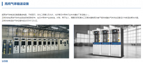
Gensun Technology semiconductor equipment parts: Gas Box demand increases, orders grow rapidly.​

Gas Box is a core component of dry process equipment, with a domestic market size of over 10 billion yuan

The Gas Box module is a modular gas supply system inside the dry process pan-semiconductor equipment. It is mainly used for gas transmission, distribution and mixing inside the equipment. It is an indispensable core component in the pan-semiconductor dry process equipment. In semiconductor process equipment, the Gas Box is mainly used for etching, thin film deposition and ion implantation equipment.

The company has a strong first-mover advantage, and the Gas Box business has entered a rapid expansion stage

Based on process synergy, the company has the first-mover advantage in entering the Gas Box field. Relying on the fluid system design and manufacturing capabilities accumulated over the years, the company began to develop fluid systems on the process equipment side in 2021. As the internal gas transmission system of the equipment, one of the core technical barriers of Gas Box is reflected in process design, and it has a strong connectivity with the external gas supply system of the equipment. The company has been deeply engaged in gas transmission systems for many years, and the underlying technologies of the external transmission system of the equipment and the internal gas system of the equipment are interconnected, which gives it a first-mover advantage in entering the Gas Box field.

The company's semiconductor equipment parts business is mainly carried out by its subsidiary Hongge Semiconductor. Gas Box includes VCR® type and Surface Mount type, which are suitable for 8-12 inch integrated circuits, flat panel displays, photovoltaic solar energy, optical fiber and microelectronics industries. The company's products have been supplied in batches to domestic leading semiconductor equipment (such as North Huachuang, Tuojing, Zhongwei, Weidao, Jingsheng, etc.) and photovoltaic cell process equipment manufacturers, and have been widely certified by domestic leading process equipment manufacturers. In 2023, revenue increased by 104% year-on-year, and new orders grew rapidly at the same time. In addition, Hongge Semiconductor continues to increase the progress of new product research and development, and is expected to achieve continuous expansion of multiple categories in the field of semiconductor equipment module components.

1717620405952.png

Please, Log in or Register to view URLs content!
 
Top