Chinese semiconductor thread II

tokenanalyst

Brigadier
Registered Member
This is the information that I have found about the possibility of a 5nm node using 193nm immersion.

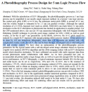
in 2019 the Shanghai ICRD released this about the possibility of a 5nm node, due stochastic EUV was not intended to be used in the FEOL <at least in this paper> due the need of high resolution pitches but the intended to be use in the metal pitches of the BEOL for what is considered at the time to be an "economical" double patterning LELE.
1717531059136.png
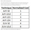
But is really economical?
the cost of DP EUV are higher than QP DUVi.
1717531577042.png
In the paper the main issue is overlay accuracy but if you can't get good overlay you can't pattern layers with EUV either. An overlay can be worked with external tools and algorithms.

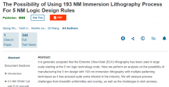
in 2023 again overlay and etching are still the main issue.
1717534708024.png

Naura and AMEC are developing more advanced etching tools.

AMEC is developing an cryogenic etching tools that could allow to etch finer HAR patterns.
1717536095828.png

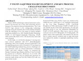
Naura etching tools have already been used for a 5nm SAQP research.

this is from 2020.
1717535853921.png
 

tonyget

Senior Member
Registered Member
Please, Log in or Register to view URLs content!

Chinese AI chip maker reduces specifications to ensure TSMC's production orders

Reuters reported, citing people familiar with the matter, that some Chinese artificial intelligence (AI) chip companies are currently designing less powerful processors so that they can continue to be produced by TSMC despite U.S. sanctions.

Sources said that the latest export controls implemented by the United States in October last year exposed China's limited advanced chip production capacity and that Chinese AI chip design companies still rely heavily on TSMC, the world's leading chip foundry.

It is reported that China's two top AI chip companies, MetaX and Enflame, submitted downgraded chip designs to TSMC at the end of last year to comply with U.S. restrictions. Shanghai-based Muxi has developed a downgraded product called the C280 and said its most advanced GPU product, the C500, was out of stock in China earlier this year.

The source also said that although China has an estimated 44 wafer foundries, only SMIC (00981) is capable of mass-producing advanced GPUs. Until recently, SMIC's production capacity was entirely reserved for Huawei.

Reports indicate that SMIC this year agreed to allocate a certain amount of production capacity to Chinese AI chip companies that are directly sanctioned by the United States and banned from overseas OEMs. One of them is Cambrian with a national background. According to sources, the United States will take restrictive measures against the company at the end of 2022, fearing that it may provide AI chip technology to the Chinese military. The company has struggled ever since.
 

european_guy

Junior Member
Registered Member
cryogenic etching tool

I was curious about this cryogenic etching thing. So I found this good article from 2018

Please, Log in or Register to view URLs content!

It is a technology developed in the '80 but never left R&D because better and more economical solutions were used like two-step Bosch process. Like the Bosch process, it is used to drill very deep and small holes, needed in 3D NAND and the key point is that at very low temperatures the chemical reactions occurring on the sidewalls of the hole are greatly reduced. Cryogenic temperature is another knob to tweak in the complex ICP RIE etching process:

“Applications are mainly deep silicon etch,” Cooke said. “Any process with mixed ion-stimulated etching and a chemical etching occurring at the same time can be tuned by adjusting the wafer temperature.”
It has some advantages over the Bosch process. “Unlike gas-chopping etch/passivation cycles, the sidewall is free of scallops,” he said.
For example, let’s say you want to etch a deep trench. In cryo etch, the ions are removing the materials in the trench until they reach the bottom, but the sidewalls remain at cryogenic temperatures. “I like to think of it as ion-assisted reactive etching. By keeping the substrate cold, only where the ions hit is where it warms up. That heat doesn’t spread out to the rest of the wafer,” Microsoft Research’s Gardner said.

Another more recent use is to allow lower-k dielectric materials and hence improved transistor performances at the same node process.

today’s low-k films have a “k value” of 2.5 or 2.6. For some time, the goal has been to reduce the “k value” to 2.2, But reducing the “k-value” is problematic. Low-k films consists of tiny pores. The pore sizes increase when the k-values fall below 2.3. As a result, the pores are prone to damage during the plasma etch process in the low-k flow.
In response, the University of Antwerp and Imec are developing a new low-k process using cryogenic etch. Initially, researchers start with a wafer equipped with low-k materials. Then, they cooled the wafer at cryogenic temperatures. “This gas may condense in the pores as liquid, which can prevent the diffusion of radicals in the interconnected pores during the subsequent plasma etching,” Zhang said.
Finally, the wafer is brought back to room temperature.


Regarding Reuters article

Please, Log in or Register to view URLs content!

reported above

Please, Log in or Register to view URLs content!

Chinese AI chip maker reduces specifications to ensure TSMC's production orders

For me, the bit of information to take away is:

Three of the four sources said SMIC agreed this year to allot a limited amount of its production capacity to Chinese AI chip firms that had been directly sanctioned by Washington and blocked from overseas production.

It seems an indirect hint at increased advanced nodes capacity at SMIC: Huawei alone is able to fully saturate SMIC advanced nodes, and if they agreed to produce for others too is maybe because they see capacity increase as a realistic target for 2024.
 

PopularScience

Senior Member
Registered Member
Please, Log in or Register to view URLs content!

Kingstone received multiple repeat orders from key wafer fab customers

Recently, Shanghai Kaishitong Semiconductor Co., Ltd. has once again received a repeat order for a low-energy, large-beam ion implanter from a 12-inch mainstream wafer fab customer. This key customer has purchased equipment from Kaishitong many times since the first quarter of last year, with a total order of more than 10 units. Since 2024, Kaishitong's ion implanter has continued to serve customers in many places for industrialized production, and the number of shipments has exceeded 10 in less than half a year. As Kaishitong's flagship product, the low-energy, large-beam ion implanter condenses many years of engineering experience and has been verified by large-scale production lines. It has high beam transmission efficiency and good stability, excellent process matching capabilities and a wide range of process coverage capabilities, and is widely favored by customers.
 

tonyget

Senior Member
Registered Member
It seems an indirect hint at increased advanced nodes capacity at SMIC: Huawei alone is able to fully saturate SMIC advanced nodes, and if they agreed to produce for others too is maybe because they see capacity increase as a realistic target for 2024.

The is no reason for SMIC to allocate all 7nm capacity to Huawei in the first place,if other companies are willing to pay the same or higher price for it. It seems to me a result of negotiation at the top
 

Hyper

Junior Member
Registered Member
The is no reason for SMIC to allocate all 7nm capacity to Huawei in the first place,if other companies are willing to pay the same or higher price for it. It seems to me a result of negotiation at the top
Top chip design firms have booked entire production capacity many times. They always and always get first preference. Apple always books the entire latest node for a year from tsmc.
 
Top