You are using an out of date browser. It may not display this or other websites correctly.
You should upgrade or use an alternative browser.
You should upgrade or use an alternative browser.
Chinese semiconductor thread II
- Thread starter vincent
- Start date
Wanye Kingstone delivered 8 ion implanters in Q1, taking new orders. Jiaxin making a etching tools for a specialty processes.
Keshitong is a domestic supplier that has achieved full coverage of the 28nm low-energy ion implantation process, and is the first to complete the verification and acceptance of the production line of domestic high-energy ion implanters.
In the first quarter of 2024, Keshitong released a large-beam ion implanter for CIS. This product received customer orders in the fourth quarter of 2023 and was delivered to customers in March 2024. In 2024Q1, Keshitong shipped a total of 8 ion implanter equipment to multiple repeat order customers, and several new customer orders were added in April. Jiaxin Semiconductor's equipment manufacturing base has been completed and put into use in November 2023, covering an area of 109 acres and a construction area of 140,000 square meters. The PHOEBUS PVD equipment independently developed by Jiaxin Semiconductor can meet the diversified process needs of customers, with both 12-inch and 8-inch architectures. In addition, Jiaxin Semiconductor spent 6-12 months developing the deep groove etching process based on the customer's special process needs.
PNC process systems, first domestic semiconductor gas tooling factory for 12 inch wafers processes.
The first fully domestically produced 12-inch wafer bulk gas supply factory in China invested and designed and constructed by the company fully meets the standards for bulk gas supply of 28 nanometers and above, successfully breaking through the international market for semiconductor-grade bulk gases. The supplier monopoly pattern has achieved zero breakthrough in domestic independent bulk gas stations at this process node.
Building three manufacturing bases for equipment, subsystems and components, two in China and one in Japan.
The second phase of the Qidong base, the Haining base and the Japanese factory were successfully opened, and the increase in production capacity has boosted the development potential of the main business. Qidong Equipment Manufacturing Base Phase II P1 plant with an area of 30,000 square meters was delivered and put into operation.
The production line was successfully constructed and has been officially put into production. Haining module and precision manufacturing base with an area of 85,000 square meters has been delivered and put into use. The equipment and machines have been successfully moved in and has been officially put into production. Overcoming the huge external About 5,000 square meters of office and factory buildings of the Japanese subsidiary, which were difficult to construct, were delivered and moved in and officially opened, providing a foundation for further development of overseas markets.
As of the end of 2023, the company has built a production and service base of 370,000 square meters, with another 70,000 square meters under construction. The company's product line layout and production capacity construction have been able to support the delivery of tens of billions of annual orders, laying the foundation for the company to achieve its 3-5 year business strategic goals. In 2024, the company expects annual new orders to be in the range of 5.5-6 billion yuan (excluding long-term orders for 5-15 years), and process equipment orders to be in the range of 1.5-2 billion yuan; with the construction of localized supply chains in the past three years, Since the task list is nearly complete, the company's process equipment delivery target is 1.3 billion yuan in 2024.
NAURA is expanding their CVD tooling line into DCVD <Dielectric Chemical Vapor Deposition> for dielectrics materials on silicon and MCVD <Modified Chemical Vapor Deposition> for photonics-communication applications
The semiconductor equipment product line continues to improve, and the platform logic is stable. The company is the leader in semiconductor equipment platform, and its products cover etching, thin film deposition, oxidation annealing, cleaning and other niche areas. It has strong market competitiveness and occupies a certain market share.
1) Etching equipment: ICP has achieved breakthroughs in 12-inch technology nodes. Polysilicon and metal etching series ICP equipment has been applied on a large scale, and multiple core processes such as shallow trench isolation etching and gate mask etching have been completed. Development and verification; CCP dielectric etching equipment has achieved coverage of multiple key processes in the fields of logic, storage, and power semiconductors; TSV etching equipment has been widely used in domestic mainstream Fab factories and advanced packaging factories, and is the leader of domestic TSV mass production lines Main machine, leading market share.
2) Thin film equipment: PVD has achieved full coverage of the metallization process of logic chips and memory chips; the layout has expanded the two major series of DCVD and MCVD products, and has achieved mass production application of more than 30 CVD products.
3) Vertical furnace and cleaning equipment:
The vertical furnace series equipment fully covers the application of logic and storage process processes. The cleaning equipment achieves full coverage of the trough process, and at the same time achieves breakthroughs in high-end single-chip processes.


interesting breakdown here of the different Kirin chip types and which devices use them. This is a rapidly growing list from Huawei in phones, tablets and PCs
looks like all the ones with L is like the downgraded/binned version
麒麟8000
1×2.40GHz + 3×2.19GHz + 4×1.84GHz
代表:nova 12 / nova 12 Pro
麒麟9000S
2×2.62GHz + 6×2.15GHz + 4×1.53GHz
代表:Mate 60 系列
麒麟9000S1 / 9000WL / 9000W
2×2.49GHz + 6×2.15GHz + 4×1.53GHz
(基于9000S超大核降频)
代表:Pura 70 / MatePad Pro 13.2 / MatePad Pro 11 2024 / MatePad 11.5"S 柔光版
麒麟9000SL / 麒麟9000WM
2×2.35GHz + 4×2.15GHz + 3×1.53GHz
(基于9000S屏蔽一大核和一小核并降频)
代表:nova 12 Ultra / MatePad 11.5"S 灵动版
麒麟9010
2×2.30GHz + 6×2.18GHz + 4×1.55GHz
(基于9000S超大核改进)
代表:Pura 70 Pro / Pro+ / Ultra
麒麟9010L
2×2.189Ghz + 4×2.18Ghz + 3×1.40Ghz
(基于9010屏蔽一大核一小核并降频)
代表:nova 12 Ultra 星耀版
looks like all the ones with L is like the downgraded/binned version
Another supplier of IBF and MRF equipment for ultra precise optics. Customers include Guowang, Castech and Changguang satellite.
For DUV lens manufacturing, first grinding/milling creates the rough shape, and then IBF and MRF polish it to the final details, with metrology at each step
Many people has this erroneous idea that is just SMEE building like 2 or 3 lithography machines on their own when in reality China is building an entire supply chain for frontend IC lithography machines.
Another supplier of IBF and MRF equipment for ultra precise optics. Customers include Guowang, Castech and Changguang satellite.
For DUV lens manufacturing, first grinding/milling creates the rough shape, and then IBF and MRF polish it to the final details, with metrology at each step

Found the company supplying vacuum tubes for euv light source. Really surprising that vacuum tubes are still used in the RF generators for EUV’s CO2 drive laser. All lower power RF generators now use solid state IGBT or GaN for amplification.

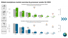
Canalys Q1 update. Again, shows here the shipment by processor vendors as well as the revenue generated by the phones sold with those process vendors.
While Apple #s dropped, it's still way ahead of everyone else. Only Hisilicon can match here in price per phone sold
QCOM still supplied some chips for HW in Q1, but I think that's mostly de-stocking older low end chips for 4G phones
Mediatek is growing.
Unisoc remains the rock bottom, low end SoC choice
If China wants to capture increasing share of revenue here, it must come from Hisilicon getting access to EUV process
