Chinese semiconductor thread II

tokenanalyst

Brigadier
Registered Member

The latest progress of Yixin Group’s advanced packaging projects

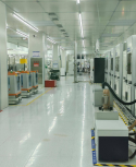
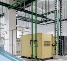
The company recently successfully completed the electromechanical engineering of the wafer-level advanced packaging project of Yixin Integrated Circuit (Yiwu) Co., Ltd., helping the project to be officially put into production.
1716214662373.png

It is understood that the project covers an area of about 70 acres, with a construction area of 49,900 square meters and a clean factory area of 25,000 square meters. It plans to produce 25,000 WLP wafer-level packaging products and 50 million SIP modules per month. Block production capacity.

As the mechanical and electrical engineering clean package of the project, Boda Construction undertook the construction and commissioning of clean decoration, pneumatic, water supply and drainage, HVAC, electric lighting, automatic control, weak current and other systems. The project was delivered on time in accordance with Party A's node requirements. The owner's equipment was moved on time in July and put into production smoothly.

Shenghejing Micro Integrated Packaging Project Starts

On May 19, according to "Jiangyin Release" news, the Shenghejing Micro ultra-high-density interconnected three-dimensional multi-chip integrated packaging project and J2C factory groundbreaking ceremony was held in Jiangyin High-tech Zone.

After the J2C factory project started this time is completed, an additional 30,000 square meters of clean room area will be added, pushing the total area of the purification factory in Shenghe Jingwei's Jiangyin operation base to more than 100,000 square meters, which will strongly support the company's three-dimensional multi-chip integrated processing and ultra- The development of projects such as high-density interconnected three-dimensional multi-chip integrated packaging meets the advanced packaging and testing service needs of customers in multiple fields such as smartphones, artificial intelligence, communications and computing, industrial and automotive electronics.

Chairman of Shenghe Jingwei said that this time the large field of view photolithography technology was used to achieve the 0.8um/0.8um line width and line spacing technical level, and the processed silicon through hole adapter board products reached 3 times the mask size. The new project marks the company's The field of advanced packaging technology has officially entered the sub-micron era.

Pangu Semiconductor’s Advanced Packaging and Testing Project Signed in Pukou


According to the "Pukou Economic Development Zone" news, on May 18, the Pangu Semiconductor advanced packaging and testing project with a total investment of 3 billion yuan was officially signed in the Pukou Economic Development Zone.

Pangu Semiconductor's advanced packaging and testing project has invested 3 billion yuan. Construction will start this year. A new factory with a total construction area of about 120,000 square meters and related ancillary facilities will be built. After reaching full production, the annual output value is expected to be no less than 900 million yuan. This project focuses on the development and application of board-level packaging technology, which will complement the weak links in Pukou's integrated circuit industry chain and enhance the level of industrial development.

Huatian Technology invested 8 billion yuan in 2018 to start the construction of the first phase of the Huatian Nanjing project. It only took 17 months from the start of construction to the start of production. Huatian Jiangsu was established in 2021 and invested 9.95 billion yuan to launch the wafer-level advanced packaging and testing production line project. The main body of the project is currently fully capped. In March this year, the company invested an additional 10 billion yuan in the second phase of the Huatian Nanjing project. Less than two months later, Pangu Semiconductor, controlled by Huatian Jiangsu, signed a contract, marking that Pukou Economic Development Zone has become the most important sector in Huatian's technology industry map.

The first phase of the advanced packaging project of Wuyuan Semiconductor has reached its peak

On May 15, according to the "North Shore Industry Alliance", the capping ceremony of the first phase of the Wuyuan Semiconductor project was successfully held.

The Wuyuan Semiconductor project is located in the North Shore chip packaging base. The project is centered around the 3D wafer stacking advanced packaging production line and is being constructed in two phases. The first phase has a total investment of 2.37 billion yuan, a total area of 122 acres, and a planned construction area of 116,000 square meters. The R&D testing plant, power plant, three-dimensional stacked plant, supporting substations, dangerous goods warehouse, etc. are expected to be completed and accepted by the end of December this year.

It is reported that Wuyuan Semiconductor provides a series of customized advanced packaging products and services based on wafer-level advanced packaging technology. A 12-inch wafer-level advanced packaging experimental line has been built, and a 12-inch wafer-level advanced packaging mass production line with a monthly production capacity of 20,000 pieces has started construction and will be put into mass production in June 2025.

 

tokenanalyst

Brigadier
Registered Member

Zhongke Feichai: It can effectively meet the needs of many domestic leading customers in the advanced packaging field in emerging technology fields such as 3D packaging and HBM. Many devices have passed verification​


What is the application status of the company's main equipment in emerging fields such as 3D packaging and HBM, whether it has obtained orders, and its future revenue contribution.

At present, the company's non-patterned wafer defect detection equipment, patterned wafer defect detection equipment, three-dimensional topography measurement equipment and other equipment have fully covered the mass production needs in the field of wafer-level advanced packaging. In this field, domestic The expansion of mainstream advanced packaging production capacity has occupied the majority of the market share and established a good product reputation and customer base.
In advanced packaging, relying on the foundation of existing products and in-depth cooperative relationships with customers, the company can effectively meet the needs of many domestic leading customers in the advanced packaging field in emerging technology fields such as 3D packaging and HBM. A variety of equipment Verified.
The future revenue contribution of these emerging fields mainly depends on the production expansion plans of downstream customers. With the company's current customer base and product base, if downstream customers have relevant production expansion needs, the company will benefit accordingly.

Please, Log in or Register to view URLs content!
 

tokenanalyst

Brigadier
Registered Member

Zhixin Semiconductor equips new energy vehicles with independent IGBTs​


After two years of research, on July 7, 2021, the production line based on the world-class 6th generation IGBT chip technology started mass production, and the first batch of independently produced automotive-grade IGBT module products in Central China officially rolled off the production line.

"The first-phase production capacity is 300,000 pieces, mainly producing 400V silicon-based IGBT modules. Compared with foreign products, the price is 50% lower, achieving a breakthrough in domestic IGBT modules from scratch." said Xu Gang, director of Zhixin Technology R&D Center.

In April this year, Zhixin Semiconductor’s second production line was put into operation with a planned production capacity of 400,000 units. It is compatible with the production of 400V silicon-based IGBT modules and 800V silicon carbide modules. The localization rate of the production line has reached 70%.

1716218476587.png1716218533234.png

1716218495819.png

Please, Log in or Register to view URLs content!
 

tokenanalyst

Brigadier
Registered Member

The School of Integrated Circuits has made important progress in the light source-mask joint optimization algorithm for high numerical aperture extreme ultraviolet lithography​


High numerical aperture (High NA, NA=0.55) extreme ultraviolet (EUV) lithography is a key technology to achieve advanced integrated circuit manufacturing for 5nm and below technology generations. Its imaging performance is limited by many factors. Light source-mask joint optimization (SMO) is an important technology to improve imaging quality in advanced lithography processes, and has been successfully applied in the 14nm and below technology generations. Therefore, establishing an SMO algorithm for High NA EUV lithography systems has clear and important practical application value.

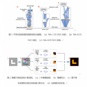
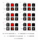
Recently, the research group of Professor Wei Yayi from the School of Integrated Circuits of the University of Chinese Academy of Sciences collaborated with the research group of Professor Ma Xu from the School of Optoelectronics of Beijing Institute of Technology to propose an SMO algorithm suitable for High NA EUV lithography systems, effectively improving the lithography system. imaging quality. First, this work established a fast lithography imaging model that takes into account the impact of the three-dimensional mask effect, deformation amplification effect, and stray light effect on the lithography imaging process in the High NA EUV lithography system. Then, through the effective combination of mask optimization technology based on the steepest descent method and light source optimization technology based on compressed sensing, the SMO algorithm is proposed. Finally, this algorithm can achieve more than 10 times improvement in computing efficiency in a GPU environment. Simulation results show that this algorithm can reduce lithography pattern errors by about 70%, significantly improve lithography imaging quality, and quickly complete optimization in about 150 seconds.​


1716235177909.png1716235234367.png

Please, Log in or Register to view URLs content!
 

Overbom

Brigadier
Registered Member
Seems this only applies for EUVs
Please, Log in or Register to view URLs content!

ASML and TSMC Can Disable Chip Machines If China Invades Taiwan​

  • Firms can remotely shut off advanced EUV chip-making machines
  • US officials concerned over risk of conflict to chip industry
ASML reassured officials about its ability to remotely disable the machines when the Dutch government met with the company on the threat, two others said. The Netherlands has run simulations on a possible invasion in order to better assess the risks, they added.
The remote shut-off applies to Netherlands-based ASML’s line of extreme ultraviolet machines, known within the industry as EUVs, for which TSMC is its single biggest client.
About the size of a city bus, an EUV requires regular servicing and updates. As part of that, the company can remotely force a shut-off which would act as a kill switch, the people said, speaking on condition of anonymity.
 

Randomuser

Senior Member
Registered Member
I wonder which region is better for semiconductors at the moment. North or south?

The hubs tend to be Beijing, Shanghai, Hefei and Shenzhen.
 
Top