Chinese semiconductor thread II

tokenanalyst

Brigadier
Registered Member

High-end parts supplier Demark Seiko Technology completed A++ round of financing​


According to Zheshang Venture Capital, Demac (Zhejiang) Precision Technology Co., Ltd. recently completed the A++ round of financing, with a financing amount of hundreds of millions of yuan, and Zheshang Venture Capital participated in the investment.

Data show that Demark Precision is a leading high-end parts supplier in China, mainly providing high-precision parts, medium and large parts and functional structural components to mid-to-high-end equipment companies in photovoltaic, wind power, semiconductor, heavy industry and other industries. The company masters the full-chain production capacity of precision parts and has accumulated deep experience in key technologies such as large structural parts welding, stress deformation control, high-precision manufacturing and surface treatment. It also has key technologies such as flatness, position tolerance, coaxiality and diameter tolerance. Leading the industry in terms of indicators. In addition, Demark Precision has about 50,000 square meters of high-standard constant-temperature workshops and nearly 100 domestic and foreign high-precision processing equipment, which can fully meet the parts delivery needs of domestic equipment manufacturers.

The semiconductor equipment and key components project of Deep Blue (Zhejiang) Precision Technology Co., Ltd. is jointly invested and constructed by Demark (Zhejiang) Precision Technology Co., Ltd. and external capital. The company is a high-tech enterprise that provides customers with professional high-precision machining business. It is located in Changxing County, Huzhou, Zhejiang Province. The existing industry-leading high-standard constant-temperature factory project has a total land area of more than 28,580 square meters, of which 125 acres will be added in the first phase, and the new construction area will be approximately 185,000 square meters. It will purchase a gantry machining center, a gantry pentahedron machining center, and a boring and milling center. Gantry machining center, precision CNC lathes and other production and auxiliary equipment will form an annual production capacity of 1,000 sets of semiconductor equipment assembly and 2,000 sets of semiconductor core components after the project is completed. The second phase will add 160 acres of land. The business scope covers semiconductor, photovoltaic, wind power, and other industries, providing one-stop technical services such as welding, precision processing, and surface spraying for medium and large parts, high-precision parts, and functional structural components of mid-to-high-end equipment.

Please, Log in or Register to view URLs content!
 

tphuang

Lieutenant General
Staff member
Super Moderator
VIP Professional
Registered Member
This is not a thread to talk about Huawei's personnel movements. I mean I tolerate some non semi posts about Huawei here, but there are better threads for it. This is a semiconductor thread.
 

tinrobert

Junior Member
Registered Member
Please, Log in or Register to view URLs content!

Naura became world’s 8th (or 9th depending on exchange rate) largest semi tool maker in 2023. Will most likely climb to 6th this year right behind KLA. I predict they’ll enter top3 by 2027
Yes I published this information on March 4, 2024. You can read it here:
Please, Log in or Register to view URLs content!
 

tokenanalyst

Brigadier
Registered Member

Jinghe Integrated's first-quarter net profit soared 123.98% year-on-year​


Domestic wafer foundry manufacturer Jinghe Integrated announced its financial report for the first quarter of 2024. It achieved operating income of 2.228 billion yuan in the quarter, a year-on-year surge of 104.44%, achieving four consecutive quarter-on-quarter growth; attributable to shareholders of listed companies The net profit was 79.26 million yuan, a year-on-year increase of 123.98%; the net profit attributable to shareholders of the listed company after deducting non-recurring gains and losses was 57.31 million yuan, a year-on-year increase of 114.87%. The gross profit margin was 24.99%, an increase of 16.97 percentage points from the same period last year, but a decrease of 3.36 percentage points from the previous quarter.

Jinghe Integration said that its operating income in the first quarter soared 104.44% year-on-year, mainly because the company continued to optimize its product structure, strengthened its technical strength, and improved its product market competitiveness. At the same time, the prosperity of the semiconductor industry rebounded, and the overall market demand recovered. Net profit and non-net profit surged by 123.98% year-on-year, mainly due to the year-on-year increase in the company's operating income during the reporting period, as well as the high level of production capacity utilization, the decrease in unit sales costs, and the year-on-year increase in product gross profit margin.

As an enterprise mainly engaged in 12-inch wafer foundry, in terms of wafer foundry process nodes, Jinghe Integration has currently achieved mass production of 150nm to 55nm process platforms and is currently developing 40nm and 28nm process platforms. In terms of process platform applications, the company currently has the technical capabilities to wafer foundry for DDIC, CIS, PMIC, MCU, Logic and other process platforms. The company's products are mainly used in smartphones, computers, flat panel displays, automotive electronics, smart home appliances, industrial control, Internet of Things and other fields.

During the reporting period, the company achieved main business income of 2.1926588 million yuan. From the perspective of application product classification, DDIC, CIS, PMIC, Logic, and MCU accounted for 71.82%, 13.27%, 8.69%, 3.48%, and 3.48% of the main business income respectively. 2.66%. The proportion of CIS in main business revenue has increased significantly and has become the company's second largest product axis.


Please, Log in or Register to view URLs content!
 

tokenanalyst

Brigadier
Registered Member

Alibaba Etian 710 actual test: the Arm architecture server chip with the best performance and energy efficiency in history​


Recently, a paper in the latest "Transactions on Cloud Computing" journal of the Institute of Electrical and Electronics Engineers (IEEE) pointed out that the Etian 710 released by Alibaba in 2021 is the Arm architecture cloud service processor with the best performance and energy efficiency today.

Alibaba Etian 710 is based on a pure 64-bit Armv9 instruction set architecture, with 128 cores, 1MB L2 cache per core, and a shared 64MB L3 cache. The highest frequency is 3.2GHz. It supports eight-channel DDR5 memory and 96 PCIe 5.0 lanes.
Alibaba claims that it is the most powerful ARM server chip in the industry, exceeding the industry benchmark by 20%, and the energy efficiency ratio has also increased by more than 50%. It is mainly used in Alibaba Cloud data centers.

This test compared a number of competing products, including Intel Xeon Platinum 8848C (32C/3.2GHz/105MB), Kunpeng 920 (60C/2.4GHz/32MB), Ampere Altra (80C/3GHz/32MB), Amazon Graviton 2/ 3(64C/2.5/2.6GHz/32MB). Among them, Intel's is naturally the x86 instruction set, and the others are all Armv8 instruction sets.

Please, Log in or Register to view URLs content!
 

tokenanalyst

Brigadier
Registered Member

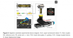
High-Precision Semiconductor Substrate Thickness Gauge Based on Spectral-Domain Interferometry​


Fujian Provincial Key Laboratory of Terahertz Functional Devices and Intelligent Sensing, School of Mechanical Engineering and Automation, Fuzhou University, Fuzhou 350116, China

Abstract​

The flatness of semiconductor substrates is an important parameter for evaluating the surface quality of semiconductor substrates. However, existing technology cannot simultaneously achieve high measurement efficiency, large-range thickness measurement, and nanometer-level measurement accuracy in the thickness measurement of semiconductor substrates. To solve the problems, we propose to apply the method that combines spectral-domain optical coherence tomography (SD-OCT) with the Hanning-windowed energy centrobaric method (HnWECM) to measure the thickness of semiconductor substrates. The method can be employed in the full-chip thickness measurement of a sapphire substrate, which has a millimeter measuring range, nanometer-level precision, and a sampling rate that can reach up to 80 kHz. In this contribution, we measured the full-chip thickness map of a sapphire substrate by using this method and analyzed the machining characteristics. The measurement results of a high-precision mechanical thickness gauge, which is widely used for thickness measurement in the wafer fabrication process, were compared with the proposed method. The difference between these two methods is 0.373%, which explains the accuracy of the applied method to some extent. The results of 10 sets of repeatability experiments on 250 measurement points show that the maximum relative standard deviation (RSD) at this point is 0.0061%, and the maximum fluctuation is 71.0 nm. The above experimental results prove that this method can achieve the high-precision thickness measurement of the sapphire substrate and is of great significance for improving the surface quality detection level of semiconductor substrates.​

1714599130082.png

Please, Log in or Register to view URLs content!
 

mst

Junior Member
Registered Member
Please, Log in or Register to view URLs content!


Taiwan semiconductor firm KYEC to exit mainland China amid geopolitical tensions, changes in cross-strait chip supply chain​

  • King Yuan Electronics Co, one of the world’s largest chip testing and packaging services firms, has divested its entire stake in a Suzhou subsidiary
  • ‘The board of directors has made a decision to withdraw from [mainland] China’s semiconductor manufacturing business,’ KYEC said
 

tokenanalyst

Brigadier
Registered Member
Please, Log in or Register to view URLs content!


Taiwan semiconductor firm KYEC to exit mainland China amid geopolitical tensions, changes in cross-strait chip supply chain​

  • King Yuan Electronics Co, one of the world’s largest chip testing and packaging services firms, has divested its entire stake in a Suzhou subsidiary
  • ‘The board of directors has made a decision to withdraw from [mainland] China’s semiconductor manufacturing business,’ KYEC said
Competition from Mainland companies was pretty much eating their business there.
 

tokenanalyst

Brigadier
Registered Member
Tongcheng New Materials ArF photoresist achieves mass shipments

Recently, Tongcheng New Materials announced that ArF photoresist has been shipped in batches.

According to reports, Tongcheng New Materials will complete the development of several ArF/ArFi photoresist products in 2023 and will have mass production capabilities. Recently, some ArF/ArFi photoresist products have passed the verification of leading domestic chip factories, obtained large-scale mass production orders, and have begun batch supply. At the same time, with the continuous deepening of new product development and customer verification, it is expected that multiple ArF/ArFi products will gradually be introduced into mass production in the second half of this year.

In 2023, Tongcheng New Materials achieved operating income of RMB 2,943.5185 million, an increase of 17.74% over the previous year, and the semiconductor photoresist business achieved operating income of RMB 201.47 million, an increase of 14.13%.​

Please, Log in or Register to view URLs content!
 
Top