Chinese semiconductor thread II

tokenanalyst

Brigadier
Registered Member

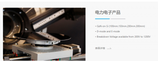
Focusing on GaN-on-Si epitaxy, Jingzhan Semiconductor and Incize carry out in-depth cooperation​

Suzhou Jingzhan Semiconductor Co., Ltd. (hereinafter referred to as "Jingzhan Semiconductor") stated that in the Einstein High-tech Park in New Leuven, Belgium, Jingzhan Semiconductor and Incize have recently reached a strategic agreement. In the memorandum of cooperation, the two parties will conduct in-depth strategic cooperation in the modeling, simulation and testing of gallium nitride on silicon (GaN-on-Si) epitaxial technology.According to reports, since 2019, Jingzhan Semiconductor and Incize have maintained close cooperation on the quality standards of GaN-on-Si epitaxy, working together to improve the quality of GaN-on-Si epitaxy to meet the demanding needs of wireless communication applications. Based on recognition of the results of cooperation, the two companies decided to formally establish a partnership to further expand and strengthen strategic cooperation and bring more innovative products to a promising and dynamic market.​

1714488581662.png

Please, Log in or Register to view URLs content!
 

tokenanalyst

Brigadier
Registered Member
GLOBALink | Schneider Electric's key production base starts construction in China
April 28, 2024

View attachment 128832

Schneider Electric Xiamen Industrial Park Friday started construction in east China's Fujian Province. After its completion, the park will become French multinational company Schneider Electric's biggest manufacturing facility for medium voltage equipment anywhere in the world. Ctto.

Please, Log in or Register to view URLs content!
just warning you now to not keep posting in wrong thread. This is for semiconductor news only. Quantum computing and medium voltage equipment do not belong here

Electrical devices and machinery -> Science and Technology Thread
Quantum Computing -> Quantum Thread or Science and Technology Threat


tokenanalyst

Brigadier
Registered Member

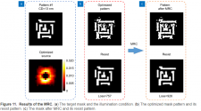
Fast source mask co-optimization method for high-NA EUV lithography​

  • EDA Center, Institute of Microelectronics of Chinese Academy of Sciences, Beijing 100029, China​
  • Key Laboratory of Photoelectronic Imaging Technology and System of Ministry of Education of China, School of Optics and Photonics, Beijing Institute of Technology, Beijing 100081, China​
  • University of Chinese Academy of Sciences, Beijing 100049, China​
  • Guangdong Greater Bay Area Applied Research Institute of Integrated Circuit and Systems, Guangzhou 510700, China​

Abstract​

Extreme ultraviolet (EUV) lithography with high numerical aperture (NA) is a future technology to manufacture the integrated circuit in sub-nanometer dimension. Meanwhile, source mask co-optimization (SMO) is an extensively used approach for advanced lithography process beyond 28 nm technology node. This work proposes a novel SMO method to improve the image fidelity of high-NA EUV lithography system. A fast high-NA EUV lithography imaging model is established first, which includes the effects of mask three-dimensional structure and anamorphic magnification. Then, this paper develops an efficient SMO method that combines the gradient-based mask optimization algorithm and the compressive-sensing-based source optimization algorithm. A mask rule check (MRC) process is further proposed to simplify the optimized mask pattern. Results illustrate that the proposed SMO method can significantly reduce the lithography patterning error, and maintain high computational efficiency.​

1714489675183.png1714489633309.png

Please, Log in or Register to view URLs content!
 

tokenanalyst

Brigadier
Registered Member

Taixing High-tech Zone Jicui Semiconductor Equipment Precision Ceramic Components Production Project "Multiple Certificates Issued"​


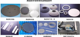
On April 28 , the precision ceramic components production project for semiconductor equipment of Jiangsu Jicui Semiconductor Ceramic Materials Research Institute in Taixing High-tech Industrial Development Zone, with a total investment of 108 million yuan, obtained the "Construction Project Quality Supervision Notice" and "Construction Project Construction" at one time Safety Approval Certificate" and "Construction Engineering Construction License" officially started construction. This project is an industrial project worth over 100 million yuan and is included in the major project tracking services of the Municipal Administrative Approval Bureau.
1714490387474.png
Jiangsu Jicui Semiconductor Ceramic Materials Research Institute is used to invest in the production of precision ceramic components for semiconductor equipment. The project is located in Taixing High-tech Zone. The factory building area is about 19,000 square meters. After completion, it can produce 20,000 ceramic components for IC equipment and 5 10,000 pieces of ceramic substrates and 100,000 pieces of ceramic bulletproof plates.

1714490507539.png

Jiangsu Jicui Semiconductor Ceramic Materials Research Institute is jointly established by the State Key Laboratory of New Ceramics and Fine Technology of Tsinghua University, Taixing High-tech Industrial Development Zone, Jiangsu Industrial Technology Research Institute, and Taizhou Industrial Technology Research Institute.

Please, Log in or Register to view URLs content!
 

aptmind

Just Hatched
Registered Member

Strengthening Controls on Semiconductor Equipment Exports to China, Japan Reportedly Tightens Export Control Measures Further​


Please, Log in or Register to view URLs content!
----
Japan is reportedly planning to expand export restrictions on four technologies related to semiconductors or quantum computing, as per
Please, Log in or Register to view URLs content!
. This move is said to represent the latest initiative in global efforts to control the transfer of strategic technologies.

The same report indicates that Japan’s new measures will affect the export of scanning electron microscopes used for analyzing nano-particle images, as well as the technology for improving semiconductor design known as Fully Depleted Silicon on Insulator (FD-SOI) technology. Japan will also require licenses for the low-temperature CMOS circuits used in quantum computers, as well as for the outputs of quantum computers themselves. These restrictions apply to Japan’s most significant trading partners, including South Korea, Singapore, and Taiwan.

This request is believed to potentially encompass exposure equipment used on silicon wafers, as well as etching equipment for three-dimensional stacking in. Among Japanese companies, Nikon and Tokyo Electron possess advanced capabilities in this field.

The same report from
Please, Log in or Register to view URLs content!
further notes that the restrictions also extend to materials related to Shin-Etsu Chemical Industries, such as photosensitive materials, and demand restrictions on exports to China. Additionally, the United States is preparing to request that the Netherlands cease providing maintenance and services for manufacturing equipment sold to China before the 2023 regulations. The strengthened control will also have a certain impact on allied countries.

Currently, Dutch company ASML is believed to still be providing such services to Chinese buyers. Per ASML’s financial report, during Q1, machine revenue from the Chinese market increased significantly from the previous quarter’s 39% to 49%.
---

These restrictions will hurt. They will cause ASML & Japanese machines to break down over time. It's delusional to think not.

Chinese policymakers need to do their best to maintain access to servicing and critical materials for as long as possible, while on the other hand fostering the replacement of as much of these critical materials & parts as possible. This balancing act is challenging; requires speaking quietly to obscure progress and prevent sanctions while also maintaining industry confidence in continued state support. If China somehow succeeds against all odds, this will be an act of industrial development never before seen in human history.
 

tokenanalyst

Brigadier
Registered Member
The same report indicates that Japan’s new measures will affect the export of scanning electron microscopes used for analyzing nano-particle images, as well as the technology for improving semiconductor design known as Fully Depleted Silicon on Insulator (FD-SOI) technology. Japan will also require licenses for the low-temperature CMOS circuits used in quantum computers, as well as for the outputs of quantum computers themselves. These restrictions apply to Japan’s most significant trading partners, including South Korea, Singapore, and Taiwan.
This is more related to quantum computing than normal semiconductor manufacturing.

These restrictions will hurt. They will cause ASML & Japanese machines to break down over time. It's delusional to think not.

Chinese policymakers need to do their best to maintain access to servicing and critical materials for as long as possible, while on the other hand fostering the replacement of as much of these critical materials & parts as possible. This balancing act is challenging; requires speaking quietly to obscure progress and prevent sanctions while also maintaining industry confidence in continued state support. If China somehow succeeds against all odds, this will be an act of industrial development never before seen in human history.
ASML machines are much more important than Japanese machines that are being replaced by Chinese players. Photoresist also is growing faster with many players now competing for the crown.

In the case of ASML I think Chinese players stockpiled enough ASML spare parts and litho machines to keep fabs working for a long time and China is very fast creating A MASSIVE lithography supply chain that should really worry ASML and Nikon. Some part of this MASSIVE supply chain is going to the refurbishing of existing lithography machines in China, for example RSLASER lasers are being made to be compatible with CYMER lasers and they stated that they are going to refurbish existent lasers in China, that same goes for optics components. Seeing this looks like ASML have increasing their production of components in China, with ZEISS opening a fabrication facility for high end optical components.

This is not an "act of industrial development never before seen in human history." in fact was expected, China has been developing semiconductors and developing their industry for quite for a long time, they have pretty advance research institutions and people who are not humanities graduates understood that and have been warning way before all this mess started that export controls in this area could only accelerate China semiconductor industry at the expense of established players in the industry.

1714496849168.png
 

european_guy

Junior Member
Registered Member
The same report indicates that Japan’s new measures will affect the export of scanning electron microscopes used for analyzing nano-particle images, as well as the technology for improving semiconductor design known as Fully Depleted Silicon on Insulator (FD-SOI) technology. Japan will also require licenses for the low-temperature CMOS circuits used in quantum computers, as well as for the outputs of quantum computers themselves. These restrictions apply to Japan’s most significant trading partners, including South Korea, Singapore, and Taiwan.

As @tokenanalyst already explained, this is just some obscure stuff, not mainstream semi equipment or materials. Practical impact of this last stunt will be zero. Maybe Japan just feels obliged to show some courtesy to US that pushed hard in these last months to have Japan materials (especially advanced photo-resist) banned but, as of today, they just got a diplomatic middle-finger....of course anything can happen in the future...

If China somehow succeeds against all odds, this will be an act of industrial development never before seen in human history.

China has succeeded already.

The virtual white flag of this tech war was raised by US in October 2023, when the new round of sanctions turned out to be a lame duck, a 200 pages of dull, bureaucratic blob. The only real thing has been forcing ASML to stop selling DUVi 28nm.

There have been no new ban extensions on US equipment (on 28nm and above), no new fronts (EDA, software, etc), no sanctions on Huawei suppliers. Mainly just raging out of frustration upon their so called "allies"....something that continues today, but the so called allies, Holland and Japan, have told US officials sent to push them: "We have suffered enough already. Let's wait until November elections, and then there will be plenty of time for new suffering in 2025".

Why TechInsights is mum about DRAM and NAND memory on the Pura 70? Why western mainstream is oddly quite mum too? They don't have the money to pay for TechInsights access? Last time it was Bloomberg that commissioned the work to TechInsights, and immediately came out with a full detailed report/article about the Mate 60, few days after phone was out.

They are mum because after they reveal that memory is Chinese (very probably, although no official confirmation yet)...they know they can only cope about it....so better to stay quiet and act like nothing happened.

China has succeeded already, the mountain pass has been crossed already, now is downhill from there...

...US is already setting up the new front line, the new trench line: exasperated protectionism, to the limit of plain import bans against Chinese chips and SME equipment, both in US and in their vassal states.
 

FairAndUnbiased

Brigadier
Registered Member
----
Japan is reportedly planning to expand export restrictions on four technologies related to semiconductors or quantum computing, as per
Please, Log in or Register to view URLs content!
. This move is said to represent the latest initiative in global efforts to control the transfer of strategic technologies.

The same report indicates that Japan’s new measures will affect the export of scanning electron microscopes used for analyzing nano-particle images, as well as the technology for improving semiconductor design known as Fully Depleted Silicon on Insulator (FD-SOI) technology. Japan will also require licenses for the low-temperature CMOS circuits used in quantum computers, as well as for the outputs of quantum computers themselves. These restrictions apply to Japan’s most significant trading partners, including South Korea, Singapore, and Taiwan.

This request is believed to potentially encompass exposure equipment used on silicon wafers, as well as etching equipment for three-dimensional stacking in. Among Japanese companies, Nikon and Tokyo Electron possess advanced capabilities in this field.

The same report from
Please, Log in or Register to view URLs content!
further notes that the restrictions also extend to materials related to Shin-Etsu Chemical Industries, such as photosensitive materials, and demand restrictions on exports to China. Additionally, the United States is preparing to request that the Netherlands cease providing maintenance and services for manufacturing equipment sold to China before the 2023 regulations. The strengthened control will also have a certain impact on allied countries.

Currently, Dutch company ASML is believed to still be providing such services to Chinese buyers. Per ASML’s financial report, during Q1, machine revenue from the Chinese market increased significantly from the previous quarter’s 39% to 49%.
---

These restrictions will hurt. They will cause ASML & Japanese machines to break down over time. It's delusional to think not.

Chinese policymakers need to do their best to maintain access to servicing and critical materials for as long as possible, while on the other hand fostering the replacement of as much of these critical materials & parts as possible. This balancing act is challenging; requires speaking quietly to obscure progress and prevent sanctions while also maintaining industry confidence in continued state support. If China somehow succeeds against all odds, this will be an act of industrial development never before seen in human history.
China already has both lab SEMs and inline metrology SEMs.
 
Top