Chinese semiconductor industry

Status
Not open for further replies.

european_guy

Junior Member
Registered Member

Zhongke Feicheng: a leading manufacturer of measuring/testing equipment, accelerating the comprehensive coverage of product lines​


Please, Log in or Register to view URLs content!

Very interesting article on
Please, Log in or Register to view URLs content!
with a lot of specific data points

China's semiconductor testing and measurement equipment market is still dominated by several foreign companies that monopolize the global market. Among them, KLM Semiconductor still has the highest share in the Chinese market, reaching 54.8%, followed by Applied Materials and Hitachi, with respective shares. are 9.0% and 7.1%

The overall performance of Zhongke Feicheng SPRUCE-600 and SPRUCE-800 equipment is equivalent to that of international competing products and has been used in It is applied in the production lines of well-known wafer manufacturers such as SMIC (verified in 2017)

In terms of coverage of testing equipment products, Zhongke Feicheng currently covers three major categories, and KLA of the United States has comprehensive coverage in 6 categories of products. in 2022, Zhongke Feicheng sold 47 non-patterned wafer defect inspection equipment.

The company currently has several pieces of equipment in its 28nm production line that have passed acceptance inspection, and another 1Xnm patternless wafer defect detection equipment is under development

The KLA Surfscan patternless wafer defect detection series of industry leader KLA covers almost all process nodes from below 5nm to above 40nm

26055832816.669544.png


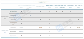
In terms of product coverage in 8 major measurement equipment fields, the American KLA company covers 6 types, and Zhongke Feicheng currently has mature coverage of 2 types of products. The prototype of Zhongke Feicei's overlay accuracy measurement equipment has been successfully developed and is waiting for customer verification; the wafer metal film measurement equipment has entered the industrialization verification stage; and the optical critical dimension measurement equipment is in the design and development stage.


Untitled.png


Revenue is growing rapidly, and the current valuation may be at a high level

In terms of finance, Zhongke Feichai achieved operating income of 238 million yuan/361 million yuan/509 million yuan/588 million yuan in 2020-2023Q1-Q3 respectively, with year-on-year growth rates of 324%/52%/41%/128% respectively;

343848697413.2685.png
 
Last edited:

tokenanalyst

Brigadier
Registered Member
One step towards chips that can work on Venus.

Jiufengshan Laboratory | Strive to achieve a comprehensive layout of silicon carbide trench device capabilities.​


Today, Jiufengshan Laboratory’s official Weibo announced that since the first batch of trench MOSFET device wafers rolled off the production line in August, Jiufengshan Laboratory has continued to overcome technical difficulties in silicon carbide processes. Recently, the laboratory has made new progress in the field of silicon carbide superjunction: it has completed the new structural design of silicon carbide multi-level trench superjunction devices with completely independent intellectual property rights . The optimized superjunction Schottky diode can achieve a resistance of more than 2000V . voltage, the specific on-resistance is as low as 0.997mΩ·c㎡ , breaking the one-dimensional limit of silicon carbide unipolar devices. At the same time, the research and development of the multi-level trench etching core process of the super-junction device has also been completed.
Jiufengshan Laboratory focuses on the research of next-generation power device technology and has formed an independent and controllable complete set of process technologies. We take you to review the technological progress released by Jiufengshan Laboratory this year:​
1703254802895.png1703254859839.png

1703254910670.png
Please, Log in or Register to view URLs content!
 

tokenanalyst

Brigadier
Registered Member

Focus on the R&D and production of semiconductor testing equipment! Nuoding Intelligent completed tens of millions of yuan in Series B financing.​


Guangzhou Nuoding Intelligent Technology Co., Ltd. (hereinafter referred to as "Nuding Intelligent"), a pan-semiconductor testing equipment R&D and production enterprise, completed tens of millions of yuan in Series B financing, funded by Shenzhen Venture Capital, Fosun Ruizheng Capital, Zhuzhou CRRC, Guxiang Fujin and old shareholder Panyu Industrial Investment Investment. This round of financing will be mainly used to expand production capacity and supplement working capital, and comprehensively strengthen talent competitive advantages and product research and development capabilities. Previously, the company has received investment from SMIC Juyuan, Kangcheng Capital, Panyu Industrial Investment and Guangzhou Fund.

Nuoding Intelligent is a modern high-tech enterprise integrating R&D and production of semiconductor testing equipment, headquartered in Guangzhou. The company's products take the passive component market in the field of special equipment as an entry point, and gradually expand from the demanding special equipment field to civilian use, expand from passive component packaging and testing to advanced semiconductor packaging and testing, and then further expand into more high-end products that are blank for domestic production. Civilian field.

1703255121075.png

According to reports, the founder of Nuoding Intelligent has ten years of development and market experience in the equipment industry, and has deep industry resources; the team was established by him, and the R&D and delivery teams have nearly 20 years of industry experience.

At present, Nuoding Intelligent has successively launched a variety of equipment such as all-in-one testing machines, ceramic packaging AOI, high-speed pin insertion machines, new energy crimping machines, chip flip-chip laminating machines, etc., which are widely used in special passive components, advanced packaging and new energy devices and other fields.

Fosun Ruizheng Capital said that there is still a lot of room for domestic substitution of China's semiconductor equipment, and there are good development opportunities for leading start-up companies in subdivided fields. He is very optimistic about the potential of domestically produced semiconductors to replace the trillion-level market, as well as the broad development space of Nuoding Intelligent in the future.

The company has accumulated deep industrial barriers in visual detection algorithms, motion control, mechanical design, electrical performance testing, etc. It can achieve the same or even better detection accuracy and detection range as foreign leading companies, with higher cost performance; and it has gathered core The team has a deep understanding of the industrial value chain for more than ten years. Fosun Ruizheng will make full use of its investment ecosystem and industrial resources to form effective synergy with its business, helping the company achieve leapfrog development.

Please, Log in or Register to view URLs content!
 

tokenanalyst

Brigadier
Registered Member

Ancai Hi-Tech: Plans to increase capital to its subsidiary to build a high-purity quartz semiconductor glass project with an annual output of 3,000 tons​


Ancai Hi-Tech announced that in order to implement the company’s strategic layout, cultivate the high-end glass industry and achieve high-quality development. Ancai Hi-Tech plans to increase capital by 51 million yuan to its wholly-owned subsidiary Henan Ancai Semiconductor Co., Ltd. (hereinafter referred to as "Ancai Semiconductor"). Ancai Semiconductor will invest in the construction of a high-purity quartz semiconductor glass project with an annual output of 3,000 tons. The total investment in the project is 199.15 million yuan.

According to disclosures, the project with an annual output of 3,000 tons of high-purity quartz semiconductor glass will build new drawing buildings, molding plants, processing plants and other buildings, and build 6 large-diameter high-purity quartz tube production lines and 12 secondary molding processing production lines. Production scale of 3,000 tons of high-purity quartz products. The construction period is 12 months, and the quartz glass project investment is 199.15 million yuan. The funding sources are self-raised funds, bank loans and other financing methods. After the project reaches full production, the average annual sales revenue is expected to be 370.88 million yuan.

Ancai Hi-Tech stated that high-purity quartz products are indispensable and important basic materials in the fields of photovoltaics and semiconductors. Their unique properties and wide range of application fields give them broad market prospects. The quartz glass project constructed through this capital increase is in line with the company's development goals and directions, can promote the company's industrial upgrading, and promote the company's high-quality development.

Please, Log in or Register to view URLs content!
 

tokenanalyst

Brigadier
Registered Member

Focusing on EDA development, Xinwushuang Simulation completed tens of millions of Pre-A rounds of financing​

Shanghai Monochip Simulation Technology Co., Ltd. (Monochip, hereinafter referred to as "Monochip") announced the successful completion of tens of millions of yuan in Pre-A round financing. This round of financing was invested by Hangshi Probe Venture Capital Partnership. This round of financing will be mainly used for core product development, team expansion and market development.
According to the data, Core Wushuang was established in May 2022. It focuses on the development of manufacturing-side integrated circuit electronic design automation (EDA) tools, actively integrates into the domestic independent chip manufacturing ecosystem, and is committed to providing reliable tools for wafer factory customers.

The company's core team is led by senior technical experts and industry figures at home and abroad. It brings together talents with backgrounds from top universities at home and abroad. It has rich experience in technology development and commercialization in the field of integrated circuit manufacturing EDA tools. Xinwushuang insists on self-developed Tuner Workbench series products. In just one and a half years since its establishment, it has launched a number of core products and has cooperated with leading wafer factories to verify and use them.

Please, Log in or Register to view URLs content!
 

tokenanalyst

Brigadier
Registered Member
CIOMP got a High Power CO2 laser patent.
1703271766927.png
In order to solve the above problems, the present invention provides a CO 2 laser power stabilization method and device for extreme ultraviolet lithography light sources, which solves the problem that the existing CO 2 laser power stabilization method needs to break the thermal balance of the laser system, through precise closed-loop control The time delay of injecting seed laser of the same frequency into the laser amplifier can significantly regulate the gain extraction efficiency of the seed laser and improve the power stability of the main pump CO 2 laser.

The invention provides a CO 2 laser power stabilization method applied to extreme ultraviolet lithography light sources . A laser amplifier with the same repetition frequency as the seed laser is used to amplify the seed laser. Without changing the discharge excitation power of the laser amplifier, Change the time delay of the seed laser entering the laser amplifier to improve the gain extraction efficiency of the seed laser.

Preferably, a certain time delay is selected, the seed laser is injected into the laser amplifier, the amplified laser pulse energy output by the laser amplifier is measured, and the amplified laser pulse energy is compared with the preset range:
When the amplified laser pulse energy is higher than the maximum value of the preset range, increase the time delay until the amplified laser pulse energy is within the preset range;
When the amplified laser pulse energy is lower than the minimum value of the preset range, the time delay is reduced until the amplified laser pulse energy is within the preset range.
A CO 2 laser power stabilization device used in extreme ultraviolet lithography light sources , including: CO 2 seed laser, CO 2 laser amplifier, control center and photodetector;
CO 2 seed laser outputs seed laser;
The CO 2 laser amplifier amplifies the power of the seed laser and outputs the amplified laser. The discharge excitation frequency of the CO 2 laser amplifier is the same as the pulse frequency of the seed laser;
The photodetector measures the pulse energy of the amplified laser and feeds the pulse energy back to the control center. The control center controls the time delay of the CO 2 seed laser output seed laser based on the relationship between the pulse energy and the preset range.

Preferably, it also includes a beam delivery unit composed of a fixed-magnification beam expander to match the beam characteristic size of the seed laser with the CO 2 laser amplifier to improve the power extraction efficiency of the CO 2 laser amplifier.
Preferably, the amplified laser is sampled through a laser sampling mirror, and the photodetector measures the pulse energy of the amplified laser
Preferably, a tin droplet target generator is also included. The tin droplet target generator generates micro-sized tin droplets with the same frequency as the CO2 seed laser, and the amplified laser interacts with the tin droplets to radiate high-efficiency EUV light .
Preferably, the control center provides trigger signals for the CO 2 seed laser, CO 2 laser amplifier and tin droplet target generator, and the time delay between each other is adjustable, and the adjustment accuracy is not less than 1 ns.
Compared with the existing technology, the present invention can achieve the following beneficial effects:
Without breaking the thermal balance of the laser system, the present invention solves the current problem of poor power stability adjustment accuracy of the main oscillation power amplifier of the pulse system, and significantly improves the stability of the power/pulse energy of the high-repetition-frequency, narrow-pulse-width CO2 laser . It meets the application requirements of high-stability EUV lithography light source for CO 2 laser power stability.

The CO 2 laser power stabilization method applied to extreme ultraviolet lithography light sources provided by the present invention mainly solves the problem that the existing CO 2 laser power stabilization method needs to break the thermal balance of the laser system. Since the laser amplifier is capable of increasing energy under repetitive frequency discharge excitation conditions, Level gas molecules relax without radiation transition. Within a pulse period, spontaneous emission, collision relaxation and other processes will occur after the discharge excitation is stopped, and the CO 2 laser gain will gradually decrease. Therefore, without changing the discharge excitation power of the laser amplifier, through precise closed-loop control of the time delay of seed laser injection of the same frequency into the laser amplifier, the seed laser gain extraction efficiency can be significantly adjusted and the stability of the main pump CO 2 laser power can be significantly improved. .
As shown in Figure 1, the embodiment of the present invention combines the CO 2 laser power stabilization method and device used in extreme ultraviolet lithography light sources. The device includes a CO 2 seed laser 1, a beam delivery unit 2, a CO 2 laser amplifier 3, Control center 4, tin droplet target generator 5, tin droplet 6, laser targeting EUV luminous area 7, laser sampling mirror 8 and photodetector 9, including:

CO 2 seed laser 1 provides high repetition frequency, narrow pulse width seed laser for the main pump CO 2 laser. It can use acousto-optic Q-switching, electro-optical Q-switching or electro-optical cavity emptying technology to achieve high repetition frequency and narrow pulse CO The output of the 2 seed laser, CO 2 seed laser 1 is controlled by the trigger signal from the control center 4.
After the CO 2 seed laser 1 outputs the seed laser, the seed laser enters the beam delivery unit 2. The beam delivery unit 2 is used to match the output beam characteristic size of the CO 2 seed laser 1 with the gain space of the CO 2 laser amplifier 3 to improve gain filling. factor, thereby effectively improving the power extraction efficiency of the CO 2 laser amplifier 3. The beam delivery unit 2 is composed of a fixed magnification beam expander.

The seed laser enters the CO 2 laser amplifier 3 for laser amplification. The CO 2 laser amplifier 3 can use radio frequency fast axial flow, radio frequency fast cross flow, radio frequency slab and other high-power laser amplifiers. The discharge excitation frequency of the CO 2 laser amplifier 3 is consistent with the seed laser. The pulse frequency is the same, or the same as the discharge excitation frequency of the CO 2 seed laser 1, and the discharge excitation duty cycle is adjustable. Under the control of the trigger signal, it can realize discharge excitation with a gate frequency of 10kHz-100kHz, and the discharge excitation duty cycle can be adjusted from 1% to 90%.
The control center 4 is used to provide precisely controllable trigger signals for the CO 2 seed laser 1, the beam delivery unit 2 and the CO 2 laser amplifier 3, and the time delay between them is precisely adjustable, and the adjustment accuracy is not less than 1 ns. Under the control sequence of the control center 4, the seed laser output by the CO 2 seed laser 1 is amplified by the CO 2 laser amplifier 3, and then lasered with the tin droplets 6 generated by the tin droplet target generator 5 in the laser targeting EUV luminous area 7 For target shooting, plasma EUV light is generated. The droplet target generator 5 uses a piezoelectric ceramic excitation capillary generator, which can spray spherical tin droplet targets with a frequency of 10kHz-100kHz and a size of 10μm-100μm. A laser sampling mirror 8 is provided on the optical path before laser target shooting. The laser sampling mirror 8 is a ZnSe material coated sampling mirror with a sampling rate of <0.2%. The laser sampling mirror 8 samples a part of the amplified seed laser, and passes this part of the sample into the high-sensitivity photodetector 9 to facilitate laser power monitoring. The photodetector 9 measures the pulse energy of the amplified laser in real time, and it comes with a fixed magnification The power attenuator avoids the energy saturation distortion of the detection signal. The photoelectric detector 9 feeds it back to the control center 4. The control center 4 performs signal collection and calculation comparison to determine the relationship between the actual measured energy value of the amplified laser pulse and the preset range. According to the energy determination result, the triggering moment of the pulse output signal of the CO 2 seed laser 1 is adjusted in real time to improve the power stability of the main pump CO 2 laser​
 

tokenanalyst

Brigadier
Registered Member

Xinhuazhang and Xinqing Technology have established in-depth cooperation to jointly develop software and hardware to accelerate car-level chip innovation.​


On December 4, system-level verification EDA solution provider Xinhuazhang officially established a strategic cooperation with Xinqing Technology, a domestic high-end automotive chip design company. The two parties have joined forces, and Xinqing Technology has introduced Xinhua Zhang related EDA verification tools to enable the collaborative development of automotive-grade chips and application software, help shorten product launch cycles on a large scale, and accelerate the innovation of new generation smart driving chips.

As China's smart car industry booms, car-grade chips have also ushered in a "golden age" of development. As the only manufacturer in China that has achieved mass production of 7-nanometer car-sized chips, Xinqing Technology's product "Longying No. 1" has been applied in many models such as Geely Lynk & Co 08 on a large scale, and has been selected into the recommended catalog of automotive chips by the Ministry of Industry and Information Technology. The company provides new options.

With the help of Xinhuazhang's automotive grade EDA verification tools, Xinqing Technology can conduct system-level software and hardware co-simulation and debugging consistent with real usage scenarios during the chip design stage, improving the performance of software and hardware synergy in system-level application environments, and reducing the cost of chips. Risks during vehicle application.

Please, Log in or Register to view URLs content!
 
Status
Not open for further replies.
Top