Chinese semiconductor industry

Status
Not open for further replies.

ZeEa5KPul

Colonel
Registered Member
All will depend on the overlay of the machine, for I have been seeing they are trying to match ASML 2nd and 3rd most advanced scanners, if they manage to match those, welp.
I wanted to stress the importance of this. Whether an immersion scanner can do 28nm, 14nm, 7nm or even 5nm is primarily a question of overlay accuracy. Doing multiple passes successfully is dependent on how accurately you can overlay the new pattern onto the already processed wafer. If the overlay accuracy is larger than the critical dimension of the feature, doing further passes is impossible.

Improving the SMEE DUVi scanners' overlay accuracy is crucial. This is where tools like the Harbin Institute's multi-axis interferometer are critical.
 

sunnymaxi

Captain
Registered Member
I would bet $1,000 on full catch up to Intel by 2028, full catch up to Samsung by 2032, and full catch up to TSMC by 2036.
Neither i m professional expert..

SMIC 7nm has 115 MTr/mm2 .. which is better than intel 7nm process.

so how can you say this, SMIC will catch up with Intel by 2028. more or less SMIC is now equivalent to intel..

1693929150277.png


as of now, only TSMC and SS is ahead. but by end of this decade, SMIC will be equivalent with TSMC..
 

tokenanalyst

Brigadier
Registered Member
I wanted to stress the importance of this. Whether an immersion scanner can do 28nm, 14nm, 7nm or even 5nm is primarily a question of overlay accuracy. Doing multiple passes successfully is dependent on how accurately you can overlay the new pattern onto the already processed wafer. If the overlay accuracy is larger than the critical dimension of the feature, doing further passes is impossible.

Improving the SMEE DUVi scanners' overlay accuracy is crucial. This is where tools like the Harbin Institute's multi-axis interferometer are critical.
I Agree, but is WAY more complex than the just the interferometers, is complicated mess of sensors and algorithms across the scanner and ASML or KLA metrology tools, it have to take into account misalignment caused by other process like planarization, etching and others. DJEL is not called a "little giant" for no reason.​
 

european_guy

Junior Member
Registered Member
I would say:

De-Americanized 14 nm logic -> Early 2025
EUV prototype -> Somewhere in 2026
DDR5 -> In 6 months. Early 2025 with a de-Americanized line
HBM -> Dependent on if they were working on it. Should follow the DDR5 shortly if they were.

Here is my attempt at this game :)

De-Americanized 14 nm logic -> Early 2025

SMIC de-americanized the 40nm line in 2022 (confirmed) and the 28nm line in 2023 (confirmed), so next steps if SMIC is able to keep the pace are 14nm in 2024 and 7nm in 2025

EUV prototype -> Somewhere in 2026

No idea here, any number is pure speculation at this point, let's wait to have some more info on this....

DDR5 -> In 6 months. Early 2025 with a de-Americanized line

I agree, CXMT road map shows Q1/Q2 2024 for DDR5

HBM -> Dependent on if they were working on it. Should follow the DDR5 shortly if they were.

I agree, key parameter of transfer speed per pin of HBM 3 is similar to DDR5, if they are secretly developing now, and this is very possible because HW needs HBM for AI, then I would be optimistic here and say HBM 3 in H2 2024.

Apart from the above I would also add:

Arfi photoresist -> 2024 in production / small batches, 2025 self-sufficiency

mask writer (e-beam or laser) -> very critical, currently all imported from Japan / Europe

materials for 14nm: wafers / mask blanks / chemicals -> hopefully the biggest part in 2024, but most difficult ones in 2025

EDA software -> Really surprised by HW here, didn't expect HW was able to design a 7nm chip. Not clear how they did it. Anyhow according to many EDA firms interviews, it seems full tool chain will be ready and validated in 2025. BTW this would be already a huge achievement!
 

LanceD23

New Member
Registered Member
Corret me if wrong,
Great news then. Even experts here like tinrobert, hvpc...etc have previously expressed doubts on CHina making any front end scanners even like basic ones let alone 28nm.
Optics is the most difficult part. NA optics for 28nm is same as smaller node.
I think its almost guarantee that China will have it own 14nm, 7nm scanners . There won't major obstacles that would block China advancement in lithography 5 or more years like before.

this would guarantee China would have per Capita over $20,000 , breaking the middle income trap.
Now, they have scale it up and for volume production.

Some people said they have ASML tools to work with now, but US officials openly expressed and banking on the wear and tear will eventually ground the current western tools China got.

So, China must overcome the difficulty of making the 28nm tool , a must...
 
Last edited:

supersnoop

Major
Registered Member
Neither i m professional expert..

SMIC 7nm has 115 MTr/mm2 .. which is better than intel 7nm process.

so how can you say this, SMIC will catch up with Intel by 2028. more or less SMIC is now equivalent to intel..

1693929150277.png


as of now, only TSMC and SS is ahead. but by end of this decade, SMIC will be equivalent with TSMC..
I think an important note is that Samsung has had production issues below 10nm
8nm poor yield at Samsung lead to loss of nVidia as a customer
7nm and below real-world thermal issues lead to loss of Qualcomm orders
Samsung is lacking the marquee customers like Apple, AMD, nVidia, Qualcomm
Now Intel Foundry is aggressively courting business, TSMC is expanding production internationally (Arizona, Japan, maybe Germany), and the Japanese government is pushing Rapidus (though like most post-90's Japanese government business initiatives, I don't expect much success, not established company, no established design support/toolchain, etc.), how much business is left? Further constraining business are the US sanctions which take all Chinese customers out of the market.
 

tokenanalyst

Brigadier
Registered Member
@tokenanalyst i remember, you have post something related domestically produced mask writer (e-beam or laser).. please repost again if possible ..
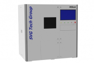
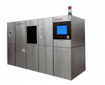
In Laser lithography for mask manufacturing they are little better off than in E-Beam lithography.
CFMEE
1703100473341.png

The LDW series of mask plate making equipment that meets the 90nm process node is the first to be launched this year​


Xinqi Micro Devices (688630.SH) recently stated when receiving a survey from institutional investors that the company has various customer categories in the pattern making field. The LDW series of mask plate making equipment that meets the 90 nanometer process node is the first to be launched this year. , has been verified on the client side; MLC and MLF models are economical and applicable small-scale mass production equipment, and their customers are mainly scientific research institutes.​

Please, Log in or Register to view URLs content!


SVGOptronics
1703100623501.png
Please, Log in or Register to view URLs content!

There was a neat company called advantools that was making very high resolution direct writing KrF excimer laser tools and they let them die.

1703101139871.png


Please, Log in or Register to view URLs content!

There also efforts from Chinese universities to achieve super resolution maskless lithography using DUV lasers.
Please, Log in or Register to view URLs content!


On the E-Beam front there is project in Beijing to develop these tools.
Everybody talks about SMEE immersion lithography machine and CIOMP CAS EUV machine but early this year the Beijing government launched the development of what I consider the most undeveloped area in the Chinese semiconductor industry, advanced E-Beam Lithography.

View attachment 121818
 

Wrought

Junior Member
Registered Member
Technical capability is all well and good, but foreign imports will continue to be necessary for long after domestic producers reach the cutting edge. Just satisfying domestic demand will take years of scaling up, and it's not like demand is standing still either.
 

CMP

Senior Member
Registered Member
Neither i m professional expert..

SMIC 7nm has 115 MTr/mm2 .. which is better than intel 7nm process.

so how can you say this, SMIC will catch up with Intel by 2028. more or less SMIC is now equivalent to intel..

1693929150277.png


as of now, only TSMC and SS is ahead. but by end of this decade, SMIC will be equivalent with TSMC..
I meant with all domestic tooling/inputs.
 
Status
Not open for further replies.
Top