Chinese semiconductor industry

Status
Not open for further replies.

ansy1968

Brigadier
Registered Member
I don't know if the N5 node will be used in Huawei's phones next year, but it's true that it's already in small-scale mass production...
N+3 transistor density of around 140MTr/mm2
Thanks bro and welcome to the forum, having knowledgeable members like you make this forum exciting. Regarding your post , SMIC maybe using ASML NXT 2050i for N+3 development and a big IF a possible domestic 7nm line in their Beijing FAB.

Semiconductor Manufacturing International Corporation (SMIC), China's leading contract chipmaker, has invested RMB 49.7 billion ($7.7 billion) in a fab in Beijing, with the first phase of the project scheduled for completion in 2024.


Please, Log in or Register to view URLs content!


Feb 23, 2021 — SMIC Jingcheng's Phase I project is currently under construction and is expected to cost approximately RMB 7.6 billion and will have a capacity ...
 

sunnymaxi

Major
Registered Member
Thanks bro and welcome to the forum, having knowledgeable members like you make this forum exciting. Regarding your post , SMIC maybe using ASML NXT 2050i for N+3 development and a big IF a possible domestic 7nm line in their Beijing FAB.

Semiconductor Manufacturing International Corporation (SMIC), China's leading contract chipmaker, has invested RMB 49.7 billion ($7.7 billion) in a fab in Beijing, with the first phase of the project scheduled for completion in 2024.


Please, Log in or Register to view URLs content!

Please, Log in or Register to view URLs content!

Please, Log in or Register to view URLs content!

Please, Log in or Register to view URLs content!


Feb 23, 2021 — SMIC Jingcheng's Phase I project is currently under construction and is expected to cost approximately RMB 7.6 billion and will have a capacity ...
14nm domestic line by next year ..

7nm domestic line will be in 2025 if all goes well ..
 

snake070

New Member
Registered Member
Thanks bro and welcome to the forum, having knowledgeable members like you make this forum exciting. Regarding your post , SMIC maybe using ASML NXT 2050i for N+3 development and a big IF a possible domestic 7nm line in their Beijing FAB.

Semiconductor Manufacturing International Corporation (SMIC), China's leading contract chipmaker, has invested RMB 49.7 billion ($7.7 billion) in a fab in Beijing, with the first phase of the project scheduled for completion in 2024.


Please, Log in or Register to view URLs content!

Please, Log in or Register to view URLs content!

Please, Log in or Register to view URLs content!

Please, Log in or Register to view URLs content!


Feb 23, 2021 — SMIC Jingcheng's Phase I project is currently under construction and is expected to cost approximately RMB 7.6 billion and will have a capacity ...
My pleasure. I read your old post about light source

From the latest papers and patents, it seems that the light source is going to replace CO2 lasers with all-solid-state lasers, which have higher power to cope with high-NA lithography. whether this is true or not, I cannot confirmed.

I believe EUV will have news by the end of 2024, since the deadline for the subject is the end of 2024.

发明名称 一种高功率EUV光刻光源的双脉冲驱动光源

本发明通过利用高功率2μm波段全固态 激光器高平均功率、高插墙效率、小装置体积等 特性,替代目前作为驱动光源的CO2激光器,获得 更高的平均功率输出,提升激发EUV辐射的功率, 解决EUV光刻机芯片产量提升的问题
 

tphuang

Lieutenant General
Staff member
Super Moderator
VIP Professional
Registered Member
by the way

The nova 12 series will go on sale directly on the 26th without a launch event, same mate60

nova12 778G 4G

nova12 pro kirin 8 or kirin 9000s 5G

nova12 ultra Kirin 9000s 5G.
I have already posted that numerous times on this thread.

I don't know if the N5 node will be used in Huawei's phones next year, but it's true that it's already in small-scale mass production...
N+3 transistor density of around 140MTr/mm2
I can assure it will not reach 140 next year. Yes, I know 定焦数码 posted N5 will be 135-140, but based on what hvpc said about CD that SMIC is working on right now, it's not sufficient for that kind of improvement. At best, you get there in 2025.
LMAO, Are you phishing? 28nm DUVI has been completed by the end of 2022, 7nm duvi will be completed in 2023

在活动自由交流环节,有学生向朱煜提问其课题组研发的工件台和ASML公司差距。朱煜回应称:目前课题组研制的工件台在大的代际上与ASML公司最先进工件台(2000系列以上产品)处于同一水平。但在小的代际上与ASML的2000系列以上产品还存在一代的差距,再迭代一次后就可以追上国际先进水平

“工件台”means the dual-stage system
Have a little respect for people on this forum.
Yes, SMIC did get awarded for validating domestic equipment of 28nm. That does not mean they have a full 28nm process
Again, SMIC does have Arfi scanner. That does not mean they have finished validating it or that they are using it in HVM. It also does not mean they are using it for 28nm process. They could very well be using it for 40nm process.

After all, ICRD started testing their SSA800 on 55nm process

Based on what Havok said before, it seems like they made some improvement to the system since early 2022 and uses planar grating laser interferometer which allows the machine to be suitable for Finfet production. However, all this remains to be tested out in practice. This is from Havok in February. Note that HIT just completed this in 2022. So the one SMIC is testing out should be able to do 14nm. In fact, internal goal of SMIC is to have fully domestic process by end of 2024.
消息人士透露,虽然比原计划推迟了2年,但是目前进展已经顺利。

大家都知道,所谓的0贰砖项的GKJ,就是28nm制程节点的GKJ。按照项目目标规定,该GKJ只能用于28nm节点,无法通过多重曝光应用于14nm节点。

虽然都是采用duv光源的浸润式原理的机器,但是14nm比28nm的机器的各项精度都要提升,其中最重要的技术难点就是GKJ内部测量的定位精度要大幅提高,因此14nmGKJ的内部测量仪器就必须从28nmGKJ的多轴激光干涉仪,升级为平面光栅激光干涉仪,只有这样才能满足掩模工件台、硅片双工件台和投影物镜之间复杂的相对位置、姿态测量需求,保证光刻机的整体套刻精度。

2023年之前,这个平面光栅激光干涉仪没有搞定,所以GKJ也就是28nm节点适用,无法更进一步提升至14nm,要等下一代改进版才行,不过,幸运的是哈工大这块去年底搞定了,原本全球GKJ巨头们都必须依赖英国和美国的平面光栅激光干涉仪,但是现在中国的光刻机不再需要了。

消息人士透露:“哈工大的这个激光干涉仪已应用在350nm至28nm的所有国产GKJ上了。”

新鲜出炉的平面光栅(极其昂贵)图:

华卓原本计划是用多轴激光干涉仪来实现符合28nm精度的双工件台,因为ASML在28nm节点的机器就是如此,到了14nm节点的时候ASML才转换到了平面光栅,可是华卓没有如同ASML那样顺利搞定,而是卡在这里相当长一段时间,华卓感觉难度很大,虽然也能最终搞定,但是必须比原计划大大的推迟了。 有了这个平面光栅,就解决了华卓的燃眉之急。 顺便也提升了双工件台和整个机器的精度,“使得目前这个28nm节点浸润式DUV光KJ,可以通过双重曝光支持14nm制程”——消息人士透露。

Having said all of this, I also wouldn't be too concerned whether or not it can do 7nm down the line. They have enough ASML scanners for that purpose.

If we are still stuck on EUV by the time SMIC have fully ramped Finfet production with ASML scanners, then we got bigger problems than we have now
 

tphuang

Lieutenant General
Staff member
Super Moderator
VIP Professional
Registered Member
My pleasure. I read your old post about light source

From the latest papers and patents, it seems that the light source is going to replace CO2 lasers with all-solid-state lasers, which have higher power to cope with high-NA lithography. whether this is true or not, I cannot confirmed.

I believe EUV will have news by the end of 2024, since the deadline for the subject is the end of 2024.

发明名称 一种高功率EUV光刻光源的双脉冲驱动光源

本发明通过利用高功率2μm波段全固态 激光器高平均功率、高插墙效率、小装置体积等 特性,替代目前作为驱动光源的CO2激光器,获得 更高的平均功率输出,提升激发EUV辐射的功率, 解决EUV光刻机芯片产量提升的问题
I think we are going to have to wait and see. Most of us are optimistic about this project due to all the patents that came out, but commercializing and industrializing it takes time.

If they can deliver 1 for testing to SMIC by 2025, that would be a great sign. It will then take SMIC some time to put it in trial production. Since domestic EUV's competition is multi-patterning ASML Arfi scanners, I'd imagine SMIC would put it into production as soon as things are stable, even if the economics aren't great
 

tokenanalyst

Brigadier
Registered Member

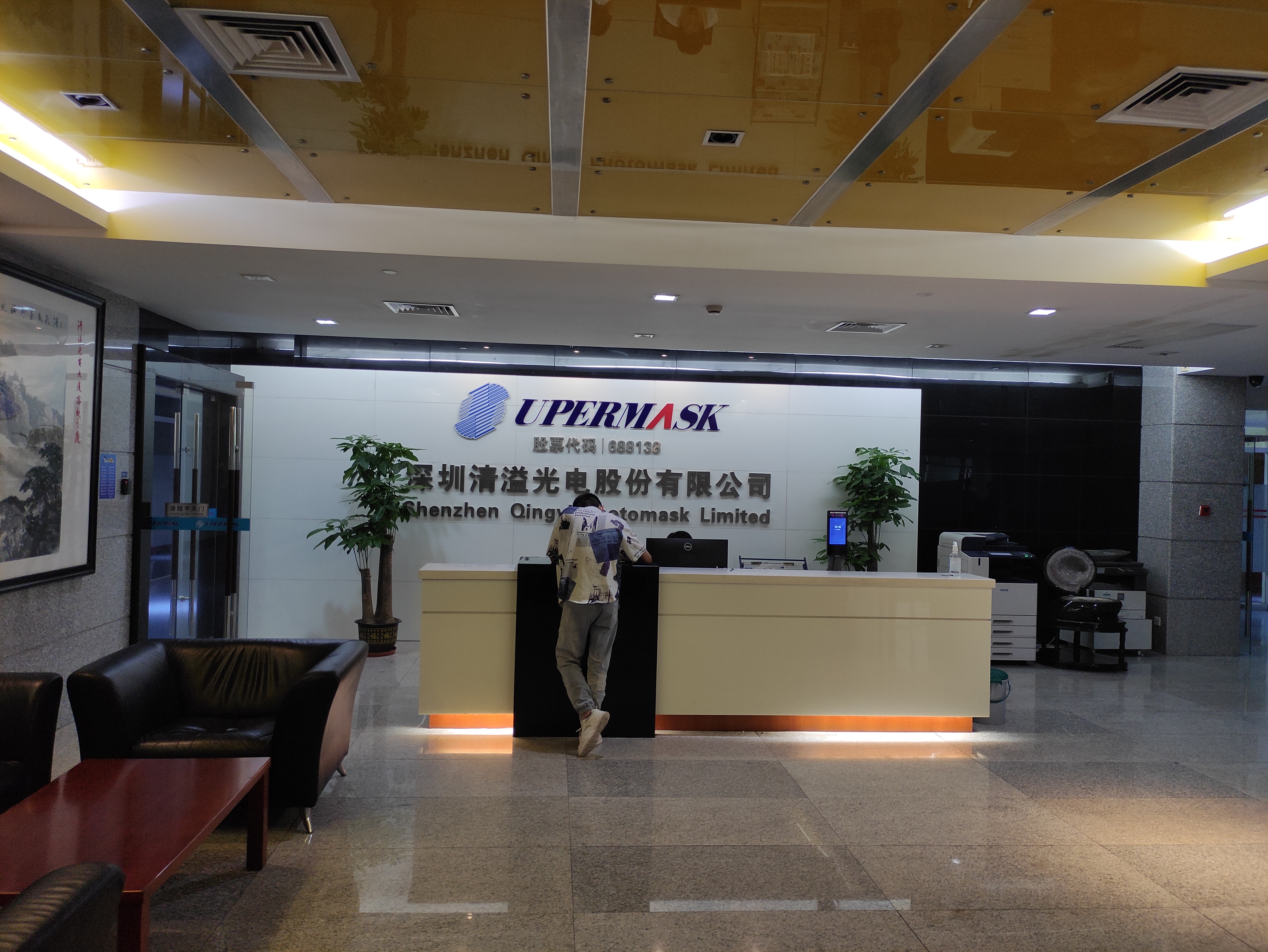
Qingyi Optoelectronics: Signed a cooperation agreement with Foshan Nanhai to accelerate the replacement of domestically produced masks​


1438098352834.375711309950966.571861.jpg

Qingyi Optoelectronics announced that the company signed a cooperation agreement with the People's Government of Nanhai District, Foshan City, Guangdong Province, and the agreement came into effect.
As of the announcement date, Foshan Qingyi Optoelectronics Co., Ltd., the implementation entity of the high-precision mask production base construction project, has been registered and established, and Guangzhou Qingyi Microelectronics Co., Ltd., the implementation entity of the high-end semiconductor mask production base construction project, is in the process of relocating to Foshan. According to relevant industrial and commercial procedures, the registered capital of Foshan Qingyi Optoelectronics Co., Ltd. is 100 million yuan (RMB), and the registered capital of Guangzhou Qingyi Microelectronics Co., Ltd. is 136 million yuan (RMB).
Qingyi Optoelectronics stated that the investment and construction of this project in Nanhai District, Foshan City, Guangdong Province aims to make full use of the comprehensive advantages of Nanhai District, Foshan City, Guangdong Province in terms of talents and resources, business environment, and industrial policy support. The investment and construction of this project will help further enhance the company's comprehensive competitive advantages and profitability, and increase the localization rate of products.
The source of funds for Qingyi Optoelectronics' external investment this time is the company's own or self-raised funds. Part of the funds the company plans to issue stocks to specific objects to raise funds and build in phases will not have an adverse impact on the company's normal production and operations. There are situations that harm the interests of the company and shareholders. This project is still in the planning and implementation stage and will not have a significant impact on the company's financial status and operating results in the short term.

Please, Log in or Register to view URLs content!
 

tphuang

Lieutenant General
Staff member
Super Moderator
VIP Professional
Registered Member
China's growing dominance in SiC substrate market going almost completely unnoticed

Please, Log in or Register to view URLs content!
科友半导体 (KY semiconductor) will be supplying 8-inch SiC wafers to a customer in Italy. Says that it's Sic Wafers are up to world leading standard

Sanan's 8-inch production has started in Hunan as we've already talked about

Please, Log in or Register to view URLs content!

Harbin govt organized an acceptance review for 8-inch SiC substrate material equipment development & industrialization

Keyou (KY semiconductor) has completed its 2023 objectives and obtained the tech/process for growing 8-inch SiC production. So really good news to see another substrate producer hitting its goals
 

interestedseal

Junior Member
Registered Member
My pleasure. I read your old post about light source

From the latest papers and patents, it seems that the light source is going to replace CO2 lasers with all-solid-state lasers, which have higher power to cope with high-NA lithography. whether this is true or not, I cannot confirmed.

I believe EUV will have news by the end of 2024, since the deadline for the subject is the end of 2024.

发明名称 一种高功率EUV光刻光源的双脉冲驱动光源

本发明通过利用高功率2μm波段全固态 激光器高平均功率、高插墙效率、小装置体积等 特性,替代目前作为驱动光源的CO2激光器,获得 更高的平均功率输出,提升激发EUV辐射的功率, 解决EUV光刻机芯片产量提升的问题
Yes, SIOM seems to be pursuing this route of 2μm wavelength solid state laser produced with Thulium doped LiYF4 crystals. I read somewhere that 2μm laser might actually have higher CE(conversion efficiency) than the current 10μm CO2 laser. Here is the link to their website that describes their research on thulium LPPEUV.
Please, Log in or Register to view URLs content!
 
Status
Not open for further replies.
Top