You are using an out of date browser. It may not display this or other websites correctly.
You should upgrade or use an alternative browser.
You should upgrade or use an alternative browser.
Chinese semiconductor industry
- Thread starter Hendrik_2000
- Start date
- Status
- Not open for further replies.
so this is basically CXMT also demonstrating 3D DRAM designs I guess. Makes sense since hvpc mentioned that aside from Huawei, CXMT and YMTC all getting into 3D DRAMI don't know if related but Huawei is developing similar technologies, looks like the use of ALD technologies is critical for these kind of nano structures.
View attachment 122513
I need to read up on this 2T0C DRAM stuff a little more
For these kind of 3D structures you need ALD equipment tools.AMC Shanghai enters PECVD market to support logic and memory chip manufacturing
The main equipment of China's first high-energy synchrotron radiation light source storage ring is installed with a closed loop, emitting light 1 trillion times brighter than the sun..
he official public account of the Institute of High Energy Physics of the Chinese Academy of Sciences that yesterday the High Energy Synchrotron Radiation Source (HEPS), a major national scientific and technological infrastructure ) The last magnet of the storage ring is installed, marking the closed loop installation of the main equipment of the HEPS storage ring.
HEPS started construction in June 2019. At present, it has completed the linear accelerator and intensifier beam extraction. The storage ring magnet, machinery, power supply, and pre-collimation system have taken the lead in completing all development tasks. Vacuum, beam control, and injection The batch processing and testing of extraction, high-frequency, low-temperature equipment and beam line stations are in progress, and the first light is expected to be launched in 2024.

The HEPS storage ring is an ultra-low emittance electron ring accelerator with a beam orbit circumference of approximately 1360.4 meters. It is the third largest light source accelerator in the world and the largest accelerator in China. The area within the ring is approximately the size of more than 20 football fields. Store high-energy and high-quality electron beams while producing synchrotron radiation. Pan Weimin, chief commander of the HEPS project, pointed out that as the core component of my country's first fourth-generation synchrotron radiation device, the storage ring is the part with the largest scale, the highest development precision, and the most difficult components of HEPS. It consists of 48 improved hybrid 7BA (7 bent iron Achromatic) magnetic focusing structure is composed of periods, each period is about 28 meters long, and contains 37 main hardware equipment such as magnets and brackets. Among them, ultra-high gradient four-pole magnets, power supply digital controllers and high-precision current sensors, high stability Magnet support and other equipment have reached the international advanced level.
Lin Guoping, chief craftsman of HEPS, said that in order to ensure accuracy and efficiency, after each system equipment has completed processing and testing, the pre-alignment unit assembly is completed in the laboratory, and the positioning accuracy of the magnets on the pre-alignment unit bracket is achieved to be better than 30 microns. It can be transported to the storage ring tunnel for installation. Depending on the number of unit magnets, each pre-alignment unit weighs about 1.7 to 8.5 tons. The installation team faced difficulties such as heavy equipment, dense tunnel equipment, and failure to affect the pre-alignment accuracy. In order to better complete the installation task, the team designed and customized a special Crane trucks and tooling, organizing process installation experiments, optimizing transportation plans, checking equipment interfaces, installation and operation spaces, and finally confirming batch installation plans, laying the foundation for efficient advancement of storage ring tunnel installation. Since the beginning of February this year, the storage ring has started to install tunnel equipment. All systems have worked closely together to dynamically adjust the installation plan according to the equipment development progress. It took 10 months to complete the entire ring with 288 pre-alignment units, 240 bent two-pole magnets, 288 Installation of main equipment such as a base to achieve a closed loop of main equipment installation.
HEPS is a major national science and technology infrastructure project approved by the National Development and Reform Commission and constructed by the Institute of High Energy Physics, Chinese Academy of Sciences. It is the core device of Beijing Huairou Science City. After completion, It will become my country's first high-energy synchrotron radiation light source, and one of the brightest fourth-generation synchrotron radiation light sources in the world, which can emit light brighter than the sun. 1 trillion times of light,helps to analyze the microstructure and evolution mechanism of matter in a deeper level, for improvement my country's national development strategy and original innovation capabilities in the field of cutting-edge basic science and technology provide a high-tech research platform.
With the development of semiconductors, Shenzhen Longtu photomask rushes to the market.
Recently, Shenzhen Longtu Mask Co., Ltd. applied to be listed on the Science and Technology Innovation Board of the Shanghai Stock Exchange and is currently in the response stage. Longtu Mask has achieved mass production of 130nm process semiconductor masks, and plans to build a 130nm-65nm high-end semiconductor mask production base through this IPO.
It plans to raise 663 million yuan for the high-end semiconductor chip mask manufacturing base project, the high-end semiconductor chip mask R&D center project and to supplement the company's working capital. According to the prospectus of Longtu Photomask, from 2020 to June 2023, its operating income was 52.6926 million yuan, 114 million yuan, 162 million yuan and 103 million yuan respectively;
Net profits were 14.4787 million yuan, 41.1642 million yuan, 64.4821 million yuan and 40.1961 million yuan respectively, showing a steady growth trend. Between 2020 and 2022, the top five customers of Longtu Photomask include Silan Micro, China Resources Micro Group, SMIC, etc. Among them, Customer A has always been its largest customer, contributing 21 million yuan in sales revenue in 2022. The sales revenue of the top five customers increased from 31.9% in 2020 to 41.65% in 2022.
In the first three quarters of this year, Longtu Photo Mask recorded revenue of 161 million yuan, a year-on-year increase of 38.59%; it achieved a net profit of 62.5548 million yuan, a year-on-year increase of 31.45%.
Using AI and a recognition rate of 90%, this SiC equipment company has achieved a new breakthrough!
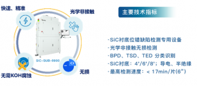
On December 12, the official Weibo of Dalian Chuangrui Spectrum Technology Co., Ltd. (hereinafter referred to as " Chuangrui Spectrum ") stated that the company has recently achieved a breakthrough in non-destructive optical detection technology for dislocation defects in silicon carbide (SiC) substrate wafers. progress , and will simultaneously launch special equipment for non-destructive testing of dislocations on SiC substrate wafers: SIC-SUB-9900 .

According to reports, the equipment is based on the principles of transient excitation and scattering spectroscopy and uses large-area optical imaging to achieve high-speed, accurate, non-contact, non-destructive optical detection of dislocation defects in SiC substrate wafers. Combined with AI recognition, it can accurately identify and classify BPD, TSD, TED and other defects in the substrate wafer (using the results of the alkali etching method widely used in the industry as a reference, the identification accuracy reaches more than 90%) .

Compared with the existing XRT (X-ray topography analysis) technology, this detection technology has significant advantages such as simple operation, fast detection speed, and high cost performance. Compared with the point scanning mode in nonlinear optical inspection, the large-area imaging method used in this equipment greatly improves the inspection speed: taking a 6-inch wafer sample as an example, the fastest inspection time is less than 17 minutes!
The number and distribution of dislocation defects such as BPD, TSD, and TED in SiC substrate wafers are important parameters that reflect the quality of the substrate. Dislocation defects in the substrate can further extend into the epitaxial layer, having a huge impact on the quality of the epitaxial layer and the final chip yield. Therefore, accurate detection, identification and statistics of dislocation defects in the substrate are extremely important aspects in substrate wafer production.
It is understood that Chuangrui Spectroscopy was founded in 2016. Based on independent technology, it has deeply cultivated the two major application fields of scientific instruments and semiconductor material testing, and has realized the empowerment of the entire industry chain from basic research to industrial production.
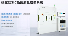
In March this year, Atheros Spectrum's SiC wafer quality large-area imaging system SiC-MAPPING532 reached the standard of sustained and stable operation and was officially shipped offline to well-known customers in the industry. This equipment is the world's first third-generation semiconductor defect detection equipment based on transient spectroscopy technology . It not only achieves fully independent domestic substitution of related technologies, but also comprehensively surpasses imported similar products in various technical indicators.
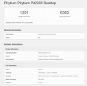
What is this? Looks a bit weird since its only 1 core. Could be a new chip with broken geekbench results or someone trolling?
Well says 8 threads.What is this? Looks a bit weird since its only 1 core. Could be a new chip with broken geekbench results or someone trolling?
Last edited:
- Status
- Not open for further replies.


