Chinese semiconductor industry

Status
Not open for further replies.

tokenanalyst

Brigadier
Registered Member
few months old news but looks relevant for the autonomous-new energy car enthusiasts here.​

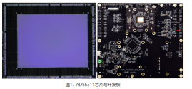
Lingming Photon officially releases ultra-high-resolution pure solid-state lidar SPAD chip ADS6311​


SPADIS area array ADS6311 chip is widely used in pure solid-state lidar fields such as vehicles and robots.
As a leading company in the SPAD dToF industry, Lingming Photonics has achieved many milestone breakthroughs in 2023, including successfully passing AEC-Q102 Grade 1 automotive certification and completing the SiPM chip production capacity increase at the hybrid solid-state lidar receiver. Pohe mass-produces goods and has been recognized by the Ministry of Industry and Information Technology as a national-level specialized, special, new and small giant enterprise, among other honors. Today, we have achieved another very exciting R&D result. The company officially released the SPADIS area array ADS6311 chip, which is widely used in pure solid-state lidar fields such as vehicles and robots!
At the upcoming 24th International Optoelectronics Expo (CIOE2023) on September 6, the company will bring silicon photon multiplier tube series (SiPM), single photon imaging array chip (SPADIS) and dToF modules, single-point and limited-point dToF Three complete product series of sensing modules were unveiled at the exhibition, and they participated in two speeches at the "Maims Micro Talk" and "Yole International Forum" to release the latest progress during the conference. We sincerely welcome and invite all industry experts and partners to visit booth 6C65 of Shenzhen International Convention and Exhibition Center for visit and guidance during the exhibition.
Product Development and Performance of ADS6311

The development process of the ADS6311 product continued the development experience and technical barriers accumulated by Lingming Photon on the area array SPADIS products. The overall development process was very smooth. The chip design will be completed and tape-out at the beginning of 2023. In July, the software and hardware system of the prototype will be developed simultaneously. At present, the Demo has been built and various functions and performance verifications have been carried out. The SPAD design and process technology used in the ADS6311 are consistent with Lingming Photonics’ SiPM process platform. SiPM is a single-point or linear array of pixels formed by connecting a large number of SPADs in parallel. Currently, the company’s SiPM products have passed AEC-Q102 Grade1 Automotive grade reliability certification and mass production, the ADS6311 based on the same process platform can also support automotive grade reliability.

Since 2018, the Lingming Photonics R&D team has been working tirelessly to iteratively develop area array products from small to large sizes. The development of the products can be traced back to the first-generation products with 80x60 and 160x120 resolutions. The previous-generation product of this series, ADS6303 (resolution 240x160) will be successfully mass-produced and shipped in July 2021. The SPADIS chip of solid-state lidar has extremely high technical barriers, including the development of high-performance SPAD devices, the design of high-speed and high-precision digital-analog hybrid circuits, the development of lidar-specific DSP, 3D stacking technology and car-grade packaging solutions, etc.

Because of this, only a few companies worldwide have developed automotive-grade SPAD chips. Through continuous technological innovation, Lingming Photon's ADS6311 chip launched this time has reached an unprecedented resolution in this product line. The photosensitive area of the chip is equipped with 768x576 SPADs, which is 4.5 times that of IMX459 and 43 times that of ibeonext. In order to improve the anti-glare characteristics and distance measurement capabilities, every 3x3 SPADs form a super pixel, thereby achieving a point cloud resolution of 256x192, which is 4.5 times that of IMX459 and 4.8 times that of ibeonext. In the current market, ADS6311 has the highest resolution One of the top pure solid-state lidar SPADIS chips.

During the development process, the smoke test and point cloud output of the ADS6311 chip were both successful, and the point cloud output also showed high-definition and stable effects, which confirmed the tireless efforts of the Lingming Photonics team during the development process. Focus and sweat. Since the initial design of the first small-size area array, the Lingming Photonics team has set the development goal of the product line. In the future, we must design the most advanced solid-state area array chip and achieve inclusive 3D sensing technology. Commercialization requires Chinese technology to lead the vigorous development of the global lidar industry. People must be ambitious and have a long way to go. Now this goal is just around the corner with the efforts of all Lingming Photon staff.

View attachment 1224981702308385054.png1702308407555.png


Please, Log in or Register to view URLs content!
 

tphuang

Lieutenant General
Staff member
Super Moderator
VIP Professional
Registered Member
Mate60pro uses Maxscend antenna tuner,as can be see on this Yole teardown

View attachment 122495
I have no question they use Maxscend or Vanchip antennas, LNAs, PAs or even SAW filters. But the question is what they are using for the 5G bands. N41 is one thing, but N77/N79 has always been the question
 

tokenanalyst

Brigadier
Registered Member

Suppressing of secondary electron diffusion for high-precision nanofabrication​


Abstract​

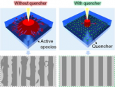
Nanopatterning is a well-established approach to fabricating nanostructures in electronics and optics, and exploiting patterning strategy to achieve smaller feature sizes and higher precision is urgently and constantly pursued. State-of-the-art extreme ultraviolet lithography and electron beam lithography have proven to produce smaller sizes. However, for such energetic radiation-based approaches, the serious diffusion behavior of the radiolytic low-energy secondary electrons will result in unpredictable defects in the unexposed matrix, limiting the ultimate resolution and hindering its potential in sub-10 nm patterning. Herein, we report significant progress in high-resolution patterning via suppressing of residues caused by secondary electron diffusion, and 10 nm line-space nanostructures are achieved by utilizing a free radical quencher in patterning a highly sensitive zirconium-containing photoresist. Lithography evaluation combined with theoretical calculation reveals this novel radical quencher approach can effectively suppress undesired electronic excitation and ionization reactions, thereby significantly improving resolution and edge roughness. By inhibiting secondary electron-induced active species, this quenching mechanism is found to increase the onset dose and effectively narrow the energy deposition; thus improving the patterning contrast and facilitating the acquisition of straight lines with sharp edges. This work provides a new perspective on active species diffusion control for higher precision nanoscale fabrication.

1702315422564.png

Conclusions​

To conclude, we have experimentally demonstrated ∼ 10 nm high-resolution patterning of alkene-functionalized ZrO2-MAA MOCs with a novel radical quencher approach, in which the radical quencher acts as an electron and radical scavenger and leads to resolution enhancement. We have successfully reproduced the high-resolution patterning under EUV and EBL. We view this novel radical quencher approach as an important step toward broad technological adoption of high-resolution patterning.

Please, Log in or Register to view URLs content!
 

sunnymaxi

Major
Registered Member

Suppressing of secondary electron diffusion for high-precision nanofabrication​


Abstract​

Nanopatterning is a well-established approach to fabricating nanostructures in electronics and optics, and exploiting patterning strategy to achieve smaller feature sizes and higher precision is urgently and constantly pursued. State-of-the-art extreme ultraviolet lithography and electron beam lithography have proven to produce smaller sizes. However, for such energetic radiation-based approaches, the serious diffusion behavior of the radiolytic low-energy secondary electrons will result in unpredictable defects in the unexposed matrix, limiting the ultimate resolution and hindering its potential in sub-10 nm patterning. Herein, we report significant progress in high-resolution patterning via suppressing of residues caused by secondary electron diffusion, and 10 nm line-space nanostructures are achieved by utilizing a free radical quencher in patterning a highly sensitive zirconium-containing photoresist. Lithography evaluation combined with theoretical calculation reveals this novel radical quencher approach can effectively suppress undesired electronic excitation and ionization reactions, thereby significantly improving resolution and edge roughness. By inhibiting secondary electron-induced active species, this quenching mechanism is found to increase the onset dose and effectively narrow the energy deposition; thus improving the patterning contrast and facilitating the acquisition of straight lines with sharp edges. This work provides a new perspective on active species diffusion control for higher precision nanoscale fabrication.

View attachment 122504

Conclusions​

To conclude, we have experimentally demonstrated ∼ 10 nm high-resolution patterning of alkene-functionalized ZrO2-MAA MOCs with a novel radical quencher approach, in which the radical quencher acts as an electron and radical scavenger and leads to resolution enhancement. We have successfully reproduced the high-resolution patterning under EUV and EBL. We view this novel radical quencher approach as an important step toward broad technological adoption of high-resolution patterning.

Please, Log in or Register to view URLs content!
@latenlazy i just saw your wow emoji on this post. please elaborate this and enhance our knowledge.. thank you
 

tokenanalyst

Brigadier
Registered Member
South Korean wafer inspection equipment manufacturer Nextin is benefiting indirectly from the US restrictions on semiconductor equipment exports to China and is accelerating its entry into the Chinese market. While on track to build a production base

The company is reportedly pouring in $200 million into a project in Wuxi High-tech Zone and Wuxi Industrial Development Group to create an advanced manufacturing and R&D base for inspection detection equipment.

Please, Log in or Register to view URLs content!

SK Nextin is expanding its production of inspection machines China. I think what is happening SK equipment companies are seeing the writing on the wall, China Semiconductor Manufacturing Equipment companies are growing quite fast, for example the inspection tool market is growing quite fast and Chinese companies like RSIC, Wuhan Jingce and others are becoming more competitive so SK companies are moving fast before the window to entry close.
 

tokenanalyst

Brigadier
Registered Member
@latenlazy i just saw your wow emoji on this post. please elaborate this and enhance our knowledge.. thank you
Secondary electrons are deal when comes to the resolution of EUV systems, as far I can understand it happens when the ultra high energy photons hit the resist, this generate electrons the affect other parts of the resist that you don't want to expose, basically speaking affect the resolution of EUV systems, so you have to manage the dosage or limit the pitch leading to the dreaded multi-patterning that seems every fab manager hates. There are some ways to deal with this but looks like Tsinghua is into something here.​

Please, Log in or Register to view URLs content!
 

latenlazy

Brigadier
@latenlazy i just saw your wow emoji on this post. please elaborate this and enhance our knowledge.. thank you
Secondary electrons are deal when comes to the resolution of EUV systems, as far I can understand it happens when the ultra high energy photons hit the resist, this generate electrons the affect other parts of the resist that you don't want to expose, basically speaking affect the resolution of EUV systems, so you have to manage the dosage or limit the pitch leading to the dreaded multi-patterning that seems every fab manager hates. There are some ways to deal with this but looks like Tsinghua is into something here.​

Please, Log in or Register to view URLs content!
Tokenanalyst’s explanation about secondary electrons is correct. General gist is that the photons are so high energy that when they get absorbed by the electrons in the resist’s molecules they actually launch the electrons out of the molecule, causing ionizing radiation which then leads to secondary interactions and thus scattershot noise. The research in the paper uses a resist with a quencher included. Quenchers are substances or materials that have high electron or radiation absorption capacity, to try to limit the free electron scattershot effects. This is not a novel approach for what it's worth, but I thought the results they got from the paper looked pretty impressive.
 

tokenanalyst

Brigadier
Registered Member

Shengjisheng Semiconductor completed a new round of financing​

according to the Science and Technology Innovation Board Daily, recently, Shengjisheng Semiconductor completed a new round of financing, and the investor was Dinghang Capital.

Shengjisheng was established in March 2018. It is a semiconductor equipment and key component R&D, production and service enterprise spearheaded by SMIC and co-sponsored by Korean Triplecores, Core Space, Xinxin Leasing and other shareholders. Shengjisheng is committed to promoting the localization of semiconductor equipment and key components, and has formed three major business segments: equipment R&D and production, key components and services, and equipment upgrading and optimization.

Ningbo Daily reported that Shengjisheng Semiconductor is committed to promoting the localization of integrated circuit equipment and key components. In the face of changes in the domestic and foreign industrial environment, it is urgent to "replenish and strengthen the chain" to target domestic industry gaps and markets. In June 2018, the Ningbo International Investment Cooperation Fair and major project signing ceremony was held. The signed projects included the Shengjisheng Semiconductor Technology Project of Shengjisheng (Ningbo) Semiconductor Technology Co., Ltd.

In September 2022, a centralized signing ceremony for the implementation of industrial projects was held in Shuyuan Town, Pudong New Area, Shanghai, including Shengjisheng’s high-end integrated circuit equipment and key component projects.

Please, Log in or Register to view URLs content!
 

snake070

New Member
Registered Member
I don't speak English, I use deepl translator

Next year or the year after. (24 or 25 ys)
SMIC and Huawei will use duv lithography to make 5nm chips

Please, Log in or Register to view URLs content!

N5 node is expected to have 140mtr/mm2

Next year there will be new Kirin 9100 soc and Kirin X1 CPU.

Tsinghua's dual-stage=NXT2000i mmo≤2.0,next version mmo≤1.5

The physical lens for EUV lithography has been developed in September 2021, the light source is still under development.

The technology freeze for EUV lithography is December 2024
 
Status
Not open for further replies.
Top