How advanced cleaning technology helps advanced nodes achieve optimal wafer yields
Semiconductor manufacturers now have new equipment that can achieve the best wafer yields. This new equipment's megasonic system uses spatial alternating phase shift (SAPS) and timed energy excited cavitation oscillation (TEBO) technology.The feature sizes of semiconductor chips are shrinking rapidly. Dynamic random access memory (DRAM) manufacturers are now producing 16GB chips in the 12nm class with a capacitor aspect ratio of 60:1. The NAND structure reaches 232 layers, and the etching aspect ratio is larger. Logic circuits are moving towards the first stage of gate-all-around (GAA) transistors at the 3nm node.
As structures become smaller and smaller, process technology becomes more challenging, making it extremely difficult to remove contamination and random defects. When feature sizes and film thicknesses reach the 10 nanometer (100 angstrom) level, even 1 nanometer (10 angstrom) particles can become fatal defects that cause transistor failure. As chip feature sizes continue to decrease below 10 nanometers, how to remove particles and other contaminants to achieve ideal yields will be a major technical challenge faced by semiconductor manufacturers.
In semiconductor fabs, where advanced photolithography, etching and deposition equipment is commonly used, wafer cleaning is sometimes considered a low-tech process. However, particles and other contaminants may change transistor characteristics, as well as contact and interconnect line resistance, and need to be removed, so wafer cleaning technology is taken to a higher level in the semiconductor manufacturing process. In fact, cleaning technology is now one of the most critical components of semiconductor production lines. In a technologically advanced factory, there may be more than 200 cleaning processes in the production process. Before each photolithography, thermal treatment or deposition process, the wafers are cleaned to remove defects and improve surface quality. The previous manual soaking system required the use of chemical solutions poured from bottles, followed by physical brushing/spraying, and a megasonic cleaning tank to remove particles. Today's cleaning systems consist of sophisticated process equipment that accurately measures and dispenses the various chemical components needed for cleaning and removes micro-contamination after etching, photolithography, chemical mechanical polishing (CMP) and other semiconductor manufacturing steps. and defects.
New generation cleaning technology

In order to solve the cleaning challenges faced by semiconductor equipment manufacturers, ACM has developed Smart Megasonix™ - a more intelligent and innovative single-wafer wet cleaning technology that can be applied to existing or future process nodes without affecting Under the condition of device characteristics, a more thorough and comprehensive cleaning can be achieved through a series of process steps. These proprietary technologies control the power intensity and distribution range of megasonic cleaning.
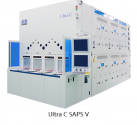
The company has developed two key technologies to enhance the cleaning capabilities of its megasonic cleaning systems. The first is Spatially Alternating Phase Shift (SAPS™) wafer cleaning technology. SAPS technology is an advanced megasonic process that uses the gap between the megasonic sensor and the wafer to change the phase of the megasonic wave. SAPS technology moves or tilts the sensor while the wafer is rotating, delivering megasonic energy evenly to every point on the wafer, even if the wafer warps.
This ensures optimal energy delivery and, when combined with appropriate dilution chemistry, creates the right environment for wafer defect removal. SAPS technology has high precision and can effectively improve the mass transfer rate during the particle removal process and the particle removal efficiency in the system. The application of SAPS technology can improve production efficiency and particle removal efficiency, thereby increasing production capacity and reducing wafer production costs.
The second innovation in megasonic technology is Timed Energy Excited Cavitation Oscillation (TEBO™) technology. Traditional megasonic technology uses the cavitation effect to create bubbles that can effectively clean. In traditional systems, these bubbles can implode or burst, destroying fine graphics. After adopting TEBO technology, the cavitation effect is more stable and no bubble implosion or rupture will occur. This enables successful removal of defects without damaging fine patterns such as DRAM's high-aspect ratio capacitors and 3D NAND's high-aspect ratio trenches and holes. The technology can also remove defects in advanced FinFET and GAA structures. As chip feature sizes continue to shrink and aspect ratios increase, the challenge of removing etch, photoresist residue, and chemical mechanical polishing particles becomes greater. Wafer features are more susceptible to damage and atomic forces are greater, making defects on the wafer surface more difficult to remove. For processing advanced nodes, new cleaning chemistries and mechanical methods are needed to remove defects that do not damage critical features. With the introduction of SAPS and TEBO technologies into megasonic systems, semiconductor manufacturers now have new tools in their quest to achieve optimal wafer yields.


