I read that article, but I'm not so sure. For one thing the machine is called L540 instead of L420. We would have to assume the L420 sold so terribly that they had a pile of millions of 9006C just waiting for L540. I find that hard to believe. Instead I believe we're looking at another Kirin 710A but at 5nm. When Huawei was first blocked from chips, Huawei and SMIC released the Kirin 710A, which was just a remake of the Kirin 710 but using SMIC processes. So it would make perfect sense for Huawei and SMIC to test 5nm production on an older chip, like the 9006C. Since it's for a low production laptop, having yield issues wouldn't be a problem. And they're selling them at about $1000 a pop so having low yield would still be profitable. They're probably doing this to ramp up for the next iteration of the mobile Kirin chip for next year or the year after. They have to reach mass production before they can announce, or release the new chip and I don't think they're there yet with 5nm, but should be some risk production at the moment which would be perfect for 9006C.
This chip was released two years ago so I suspect this is left over stock from TSMC.
Article from 2 years ago covering the same laptop.

You are using an out of date browser. It may not display this or other websites correctly.
You should upgrade or use an alternative browser.
You should upgrade or use an alternative browser.
Chinese semiconductor industry
- Thread starter Hendrik_2000
- Start date
- Status
- Not open for further replies.
I don't find it hard to believe at all.I read that article, but I'm not so sure. For one thing the machine is called L540 instead of L420. We would have to assume the L420 sold so terribly that they had a pile of millions of 9006C just waiting for L540. I find that hard to believe. Instead I believe we're looking at another Kirin 710A but at 5nm. When Huawei was first blocked from chips, Huawei and SMIC released the Kirin 710A, which was just a remake of the Kirin 710 but using SMIC processes. So it would make perfect sense for Huawei and SMIC to test 5nm production on an older chip, like the 9006C. Since it's for a low production laptop, having yield issues wouldn't be a problem. And they're selling them at about $1000 a pop so having low yield would still be profitable. They're probably doing this to ramp up for the next iteration of the mobile Kirin chip for next year or the year after. They have to reach mass production before they can announce, or release the new chip and I don't think they're there yet with 5nm, but should be some risk production at the moment which would be perfect for 9006C.
ARM laptops (excluding Apple) have always been poor sellers. The performance is just lacking in comparison to Intel (and AMD) laptops. 8GB of RAM for a $1000 USD laptop is highway robbery. You can get a low mid-range Lenovo with 16GB of RAM for less than that and that's OUTSIDE China. I would imagine that prices inside China would be better.
Recent new actions of two domestic SiC testing equipment companies
The booming development of the semiconductor field has boosted the rise of the domestic semiconductor testing equipment industry, and related companies have received good news about financing and product delivery.
Recently, Suzhou Geize Precision Technology Company successfully completed a round of tens of millions of yuan in financing, benefiting from Su Venture Capital, Guofa Venture Capital, Su Gaoxin Rongsheng, Yuanhe Origin, Zehe Venture Capital, Zhuoyuan Capital and other parties support from investment institutions. The main purpose of this financing will be used for the expansion of the company's team, the research and development of new products and market expansion, and to further promote the in-depth development of semiconductor testing equipment and high-end sensing products. GEZE Technology focuses on the research and development of semiconductor optical quality inspection equipment and industrial intelligent optical sensing products, which are widely used in wafer manufacturing, chip manufacturing, advanced packaging and other fields.
At the same time, semiconductor testing equipment manufacturer Urupu has also made new progress. The company successfully delivered a film thickness measurement device, Eos200DSR, which is compatible with 8/6-inch wafer size and used to measure the thickness of multiple layers of films of different materials on the surface of SOI (Silicon-On-Insulator) wafers. Eos200DSR has a wide range of applications and can be used to measure the thickness of silicon dioxide (BOX) and top layer silicon. It is also suitable for thin film measurement needs of other materials such as silicon-based lithium niobate.
Gechuang Dongzhi: Building a full-stack domestic semiconductor CIM solution based on a new perspective
As semiconductor manufacturing processes and quality requirements continue to improve, more and more semiconductor manufacturers are realizing the importance of digital transformation and need a complete and stable CIM solution to control process quality and improve product yield. The CIM system is known as the "EDA of semiconductor manufacturing" and is a life-level system for semiconductor manufacturing. However, it is still dominated by foreign giants. Therefore, domestic substitution in this field is particularly important. Gechuang Dongzhi is one of the representative manufacturers. .
Gechuang Dongzhi was founded in 2018 by TCL strategic incubation. With the mission of "making industry smarter", it is committed to the R&D, design and application innovation of domestic industrial software to help the construction and practice of China's Industry 4.0.
Based on TCL's 40 years of smart manufacturing genes, Gechuang Dongzhi has created a national-level dual-span industrial Internet platform originating from the semiconductor manufacturing industry (certified by the Ministry of Industry and Information Technology, ranking TOP10 in 2023), using AI, Internet of Things, big data, digital twins, etc. Core technology provides one-stop solutions from edge data collection, industrial big data analysis to top-level application development, including production control, equipment management, quality optimization, energy and carbon management, supply chain services, warehousing and logistics, etc., for semiconductors, new technologies More than 20 industries and 20,000+ companies, including energy, automobiles, and 3C electronics, provide digital transformation services.
In the field of smart manufacturing in the semiconductor industry, Gechuangdongzhi has built a full-stack domestic CIM overall solution for semiconductor smart factories based on a new perspective of "production-analysis-prediction", including: MES manufacturing execution system, EAP equipment automation system, RCM Machine remote control management system, APC advanced process control system, SPC statistical process control system, FDC fault detection and classification system, MFA multi-factor analysis system, ADC intelligent detection system, QMS quality management system, LIMS laboratory management system, RMS Process recipe management system, MCS material handling system, CMS central equipment status monitoring system, big data middle platform and other products can help semiconductor companies achieve transparent production execution, automated equipment management, high-efficiency plan collaboration, accurate quality traceability and logistics management, etc. Increase production capacity, reduce losses, improve yield, and optimize production and process design. It has served customers in the semiconductor industry such as SMIC, SAIC Infineon, Wuhan Xinxin, Zhuzhou CRRC, Yangjie Technology, Li Auto-Sko Semiconductor, etc.
Northern Huachuang discloses patents related to "etching methods and semiconductor process equipment"
Tianyancha shows that Northern Huachuang has recently added several pieces of patent information, one of which is titled "An etching method and semiconductor process equipment for a silicon-containing organic dielectric layer" with the public number CN117174582A.
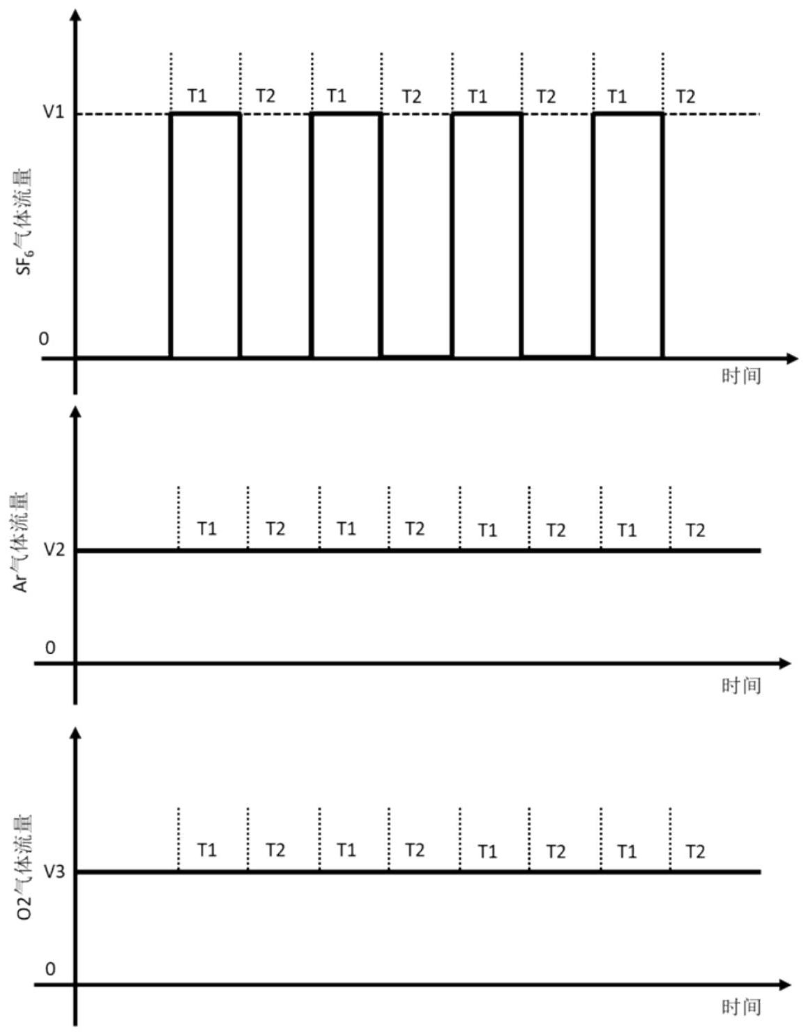
The patent abstract shows that the present invention discloses an etching method and semiconductor process equipment for a silicon-containing organic dielectric layer. The silicon-containing organic dielectric layer is etched by using at least two alternate etching steps, wherein at least two etching steps are used. The etching step includes a first etching step and a second etching step. The etching gas used in the first etching step at least includes an oxygen-containing gas. The etching gas used in the second etching step at least includes an oxygen-containing gas and a gas containing oxygen. Fluorine gas, so that the first etching step and the second etching step can be alternately performed through cycles, the gas ratio of oxygen-containing gas and fluorine-containing gas can be adjusted, and the etching rates of different elements in the silicon-containing organic dielectric layer can be adjusted. This can further reduce micro-grooves or protrusions at the bottom of trenches or through-holes in the silicon-containing organic dielectric layer, so that the bottom of the trench or via-hole has a smooth topography, thereby avoiding electric field stress at the bottom of the trench or via-hole. Too much concentration affects the performance of electronic devices.
It is reported that in the field of semiconductor process equipment, North Huachuang's main products include etching, thin film, cleaning, heat treatment, crystal growth and other core process equipment, which are widely used in logic devices, memory devices, advanced packaging, third-generation semiconductors, and semiconductor lighting. , micro-electromechanical systems, new displays, new energy photovoltaics, substrate materials and other manufacturing processes.
China government puts all hope on Huawei to lead the country on semiconductor and tech independence.
It hands $30billion investment fund to huawei. Probably large chunk as subsidies for SMIC for manufacturing chips for Huawei until more cost effective tools come.
It hands $30billion investment fund to huawei. Probably large chunk as subsidies for SMIC for manufacturing chips for Huawei until more cost effective tools come.
Taiwan, China, announces a list of core key technologies: 14nm and below chip manufacturing, advanced packaging, etc. are prohibited from being obtained by mainland China
The list of 22 core key technologies announced that day was submitted to the administrative department of Taiwan, China after collecting opinions and discussions from all parties.
18. Chip (IC) manufacturing technology for 14nm and below processes and its key gases, chemicals and equipment technologies
Here we go, this is the first attempt at banning all the materials for advanced processes. I'm afraid it won't remain the only one.
US is now clearly pushing their "allies" to extend bans on materials, next stop will be Japan...I read this today news as an anticipation of what we will see much more broadly in 2024.
SMIC, YMTC and CXMT, the key companies that are the main target of the attack, have to fully localize silicon wafers and chemicals (including photoresists) for their advanced products within 2024.
US today has revealed what will be their next target. It's a race against time now.
Last edited:
Imagine, Biden could have done this last year when he first imposed the sanctions. If the intention was to hurt China's A.I growth as much as possible, that would have been the logical way. He could have issued an executive order, the allies Taiwan, Korea, Netherlands and Japan would have made some minor protest and then all would have caved in.Taiwan, China, announces a list of core key technologies: 14nm and below chip manufacturing, advanced packaging, etc. are prohibited from being obtained by mainland China
Here we go, this is the first attempt at banning all the materials for advanced processes. I'm afraid it won't remain the only one.
US is now clearly pushing their "allies" to extend bans on materials, next stop will be Japan...I read this today news as an anticipation of what we will see much more broadly in 2024.
SMIC, YMTC and CXMT, the key companies that are the main target of the attack, have to fully localize silicon wafers and chemicals (including photoresists) for their advanced products within 2024.
US today has revealed what will be their next target. It's a race against time now.
China has had a free 1 year pass. It is very likely they have put it to good use and prepared accordingly including counter sanctions on critical raw materials.
I mean this is Taiwan we are talking about here. what do they possibly have for 14nm manufacturing tech that the mainland does not?Taiwan, China, announces a list of core key technologies: 14nm and below chip manufacturing, advanced packaging, etc. are prohibited from being obtained by mainland China
Here we go, this is the first attempt at banning all the materials for advanced processes. I'm afraid it won't remain the only one.
US is now clearly pushing their "allies" to extend bans on materials, next stop will be Japan...I read this today news as an anticipation of what we will see much more broadly in 2024.
SMIC, YMTC and CXMT, the key companies that are the main target of the attack, have to fully localize silicon wafers and chemicals (including photoresists) for their advanced products within 2024.
US today has revealed what will be their next target. It's a race against time now.
It's just nonsense
Taiwan, China, announces a list of core key technologies: 14nm and below chip manufacturing, advanced packaging, etc. are prohibited from being obtained by mainland China
Here we go, this is the first attempt at banning all the materials for advanced processes. I'm afraid it won't remain the only one.
US is now clearly pushing their "allies" to extend bans on materials, next stop will be Japan...I read this today news as an anticipation of what we will see much more broadly in 2024.
SMIC, YMTC and CXMT, the key companies that are the main target of the attack, have to fully localize silicon wafers and chemicals (including photoresists) for their advanced products within 2024.
US today has revealed what will be their next target. It's a race against time now.
Yes are guest the the people who work at mainland China gas semiconductor companies like Nata and Jinhong are pretty sad knowing that their competition is just leaving them a huge market like China. But the main issue is that with semiconductor materials with the exception of probably photoresist, there is not clear cut between 20nm process and below 14nm, a gas is a gas, I don't know, maybe purity? but what will stop a company buying a semiconductor grade gas for one process and then purify it for a more advanced process. I term of equipment that Island as much as SK are even way more dependent on US and Japan than mainland China so there is not much to it in that regard and most of the equipment they sell is for more mature process.
- Status
- Not open for further replies.