Poor Dutch can't say no to the US and is given a lousy reason why the ban is necessary.
(Bloomberg) -- China’s Semiconductor Manufacturing International Corp. used equipment from ASML Holding NV to manufacture an advanced processor for a Chinese smartphone that alarmed the US, according to people familiar with the matter.
In a suggestion that export restrictions on Europe’s most valuable tech company may have come too late to stem China’s advances in chipmaking, ASML’s so-called immersion deep ultraviolet machines were used in combination with tools from other companies to make the Huawei Technologies Co. chip, the people said, asking not to be identified discussing information that’s not public.
ASML declined to comment. There is no suggestion that their sales violated export restrictions.
The firm’s shares dropped as much as 2.1% in Amsterdam after the report, and were trading 0.6% lower at €558.5 apiece as of 3:54 p.m. local time.
The US has been working with Japan and the Netherlands to prevent China from accessing advanced semiconductor technology of the kind demonstrated in the 7-nanometer chip that powers Huawei’s Mate 60 Pro, in order to curb the country’s technological advancement and prevent it from gaining a military edge.
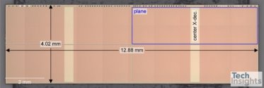
Despite those broad restrictions, Huawei surprised the world in August when it quietly introduced its new smartphone with 5G capabilities and a cutting-edge processor. A teardown of the device conducted by TechInsights for Bloomberg News revealed the chip was produced by SMIC, demonstrating manufacturing capabilities well beyond where the US had sought to stop China’s advance.
That prompted questions both about how SMIC was able to manufacture the chip, and the effectiveness of the Washington-led controls. SMIC didn’t respond to a request for comment.
New Controls
ASML occupies a pivotal role in the global chip supply chain. It has a monopoly on advanced extreme ultraviolet lithography systems, or EUVs, that are indispensable to the production of the most cutting-edge chips, and it also supplies the deep ultraviolet lithography machines needed to make more mature semiconductors.
Read More: ASML, Europe’s Most Valuable Tech Firm, Defines Global Chip War
ASML has never been able to sell its EUV machines to China because of export restrictions. But less advanced DUV models can be retooled with deposition and etching gear to produce 7-nanometer and possibly even more advanced chips, according to industry analysts. The process is much more expensive than using EUV, making it very difficult to scale production in a competitive market environment.
In China, however, the government is willing to shoulder a significant portion of chipmaking costs.
Chinese companies have been legally stockpiling DUV gear for years — especially after the US introduced its initial export controls last year before getting Japan and the Netherlands on board.
Pressure from President Joe Biden’s administration pushed the Dutch government last summer to announce plans to prohibit ASML from shipping three out of four of its most advanced-model immersion DUV lithography machines, its second-most capable category of machinery, to China without a license. ASML is still able to export those products to China at the moment but the shipments will be prohibited from January.
According to an investor presentation published by the company last week, ASML experienced a jump in business from China this year as chipmakers there boosted orders ahead of the export controls taking full effect in 2024. China accounted for 46% of ASML’s sales in the third quarter, compared with 24% in the previous quarter and 8% in the three months ending in March.
New controls that the Biden administration announced this month further limit the exports of DUV machines.
The regulations use a unilateral authority called a de minimis rule to control the sale of specified foreign-made lithography machines that contain any amount of American materials, said Stephen Bartenstein and Peter Lichtenbaum, export control attorneys at Covington & Burling LLP, without commenting on the companies affected.
ASML Chief Executive Officer Peter Wennink told investors last week that together, the new US and Dutch curbs will affect up to 15% of the firm’s sales in China.
Under the new rules, ASML can still ship its less advanced NXT:1980Di machine to Chinese facilities that make older chips, according to Wennink. But it can’t sell to fabs that produce semiconductors near the cutting edge.
That rule affects ASML shipments to six fabs in China, according to people familiar the matter — including one SMIC facility. It’s unclear whether that is the facility that produced the 7-nanometer chip for Huawei, and the US Bureau of Industry and Security did not respond to questions on the matter.
Unilateral Move
Broadly speaking, the new US curbs bring the country’s equipment restrictions in line with those of the Netherlands, according to several industry experts.
But the regulation of immersion DUV machines is one area where the US went further than its ally, in a move that risks being seen as extraterritorial bullying.
A senior Dutch official confirmed that the Netherlands’ government was informed by the US about the Oct. 17 measures. But that doesn’t mean the move went over well: A group of Dutch politicians, including lawmakers from two parties in the ruling coalition, called for their government to take a stand against the new US measures.
“Unilaterally changing the rules during a contest where competitiveness and strategic autonomy are at stake is difficult to accept, even by a good ally,” said Dutch Christian Democrat lawmaker Mustafa Amhaouch earlier this week.
ASML CEO Wennink also publicly opposed the measures and warned they might encourage China to develop competing technology. “The more you put them under pressure, the more likely it is that they will double up their efforts,” he said in a January interview with Bloomberg News.
“The United States has made a different security analysis. They are free to do so,” Dutch Foreign Trade Minister Leisje Schreinemacher said in the parliament this week. But she also said she believes the European Union should have a greater role in discussions with the US on export controls for sensitive technology and that she will bring this issue up with Prime Minister Mark Rutte in Brussels. 


