I’m telling you overlay accuracy is one of those improvements that makes it easier for the other areas.I think it's natural to go there over time. But there are many areas of improvement and improving overlay precision is just one of them. There are many factors that contribute to system up time & yield for a lithography system. I don't pretend that I'm involved in this and would know all those factors. I would presume that overlay accuracy is one of those factors, but I just want to see the system get put into usage and improve rather than being more interested in improving overlay over other area
You are using an out of date browser. It may not display this or other websites correctly.
You should upgrade or use an alternative browser.
You should upgrade or use an alternative browser.
Chinese semiconductor industry
- Thread starter Hendrik_2000
- Start date
- Status
- Not open for further replies.
I see that, but there are also plenty of other things you will need to focus on.I’m telling you overlay accuracy is one of those improvements that makes it easier for the other areas.
For example, system uptime and system usability are things I would consider are things that any new product should improve first.
Those are standard product and service support engineering from NPI (new product introduction). They don’t take resources from R&D.I see that, but there are also plenty of other things you will need to focus on.
For example, system uptime and system usability are things I would consider are things that any new product should improve first.
Last edited:
I completely disagree that product uptime does not take resources from r&dThose are standard product and service support engineering from NPI (new product introduction). They don’t take resources from R&D.
Product uptime improvement is not R&D side engineering. It’s production and service engineering. Very different part of any hardware company’s org chart.I completely disagree that product uptime does not take resources from r&d
Effective multi-objective inverse lithography technology at full-field and full-chip levels with a hybrid dynamic priority algorithm.
Key Laboratory of Photoelectronic Imaging Technology and System of Ministry of Education of China, School of Optics and Photonics, Beijing Institute of Technology, Beijing 100081, China
Abstract
Inverse lithography technology (ILT), such as source mask optimization (SMO), is used to improve lithography performance. Usually, a single objective cost function is selected in ILT, and an optimal structure for one field point is achieved. The optimal structure is not the case for other images at full field points where the aberrations of the lithography system are different, even in high-quality lithography tools. The optimal structure that must match the high-performance images at the full field is urgently required for extreme ultraviolet lithography (EUVL). In contrast, multi-objective optimization algorithms (MOAs) limit the application of multi-objective ILT. Assigning target priority is incomplete in current MOAs, which results in the over-optimization of some targets and under-optimization of others. In this study, multi-objective ILT and a hybrid dynamic priority (HDP) algorithm were investigated and developed. High-performance images with high fidelity and high uniformity were obtained at multi-field and multi-clip areas across the die. A hybrid criterion was developed for the completion and reasonable prioritization of each target to ensure sufficient improvement. Compared to the current MOAs, the uniformity of images at full-field points was improved by up to 31.1% by the HDP algorithm in the case of multi-field wavefront error-aware SMO. The multi-clip source optimization (SO) problem showed the universality of the HDP algorithm to deal with different ILT problems. It acquired higher imaging uniformity than existing MOAs, which indicated that the HDP is more qualified for multi-objective ILT optimization than existing MOAs.


You know I wonder if LPP light sources have limitations with applying this kind of algorithmic scanning optimization.
Effective multi-objective inverse lithography technology at full-field and full-chip levels with a hybrid dynamic priority algorithm.Key Laboratory of Photoelectronic Imaging Technology and System of Ministry of Education of China, School of Optics and Photonics, Beijing Institute of Technology, Beijing 100081, China
AbstractInverse lithography technology (ILT), such as source mask optimization (SMO), is used to improve lithography performance. Usually, a single objective cost function is selected in ILT, and an optimal structure for one field point is achieved. The optimal structure is not the case for other images at full field points where the aberrations of the lithography system are different, even in high-quality lithography tools. The optimal structure that must match the high-performance images at the full field is urgently required for extreme ultraviolet lithography (EUVL). In contrast, multi-objective optimization algorithms (MOAs) limit the application of multi-objective ILT. Assigning target priority is incomplete in current MOAs, which results in the over-optimization of some targets and under-optimization of others. In this study, multi-objective ILT and a hybrid dynamic priority (HDP) algorithm were investigated and developed. High-performance images with high fidelity and high uniformity were obtained at multi-field and multi-clip areas across the die. A hybrid criterion was developed for the completion and reasonable prioritization of each target to ensure sufficient improvement. Compared to the current MOAs, the uniformity of images at full-field points was improved by up to 31.1% by the HDP algorithm in the case of multi-field wavefront error-aware SMO. The multi-clip source optimization (SO) problem showed the universality of the HDP algorithm to deal with different ILT problems. It acquired higher imaging uniformity than existing MOAs, which indicated that the HDP is more qualified for multi-objective ILT optimization than existing MOAs.
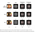
View attachment 120322
One question I have about US sanctions is, it says it does not target consumer tech that is commodity level or common. So, Huawei for example still produces laptops with Windows and other Microsoft software without any problems.
Why is it that Android and Google services with GMS and Playstore is banned for Huawei? These should be equally consumer level as well and Huawei should have been able to use it. Or is it because Google wanted kill Huawei and used the sanctions as an excuse to ban Huawei.
Why is it that Android and Google services with GMS and Playstore is banned for Huawei? These should be equally consumer level as well and Huawei should have been able to use it. Or is it because Google wanted kill Huawei and used the sanctions as an excuse to ban Huawei.
Computation lithography and mask optimizations are needed regardless the light source to get the best resolution for advanced process nodes, maybe will be a less of a necessity with FELs and SSMBs.You know I wonder if LPP light sources have limitations with applying this kind of algorithmic scanning optimization.
- Status
- Not open for further replies.
