Delusions of politicians who never had to train a ML model in their life.Can someone be in the shoe of the US and explain to me why trying to ban "advanced" AI chips which are basically glorified GPU's going to prevent China from developing AI and be competitive with US AI models?
1. Machine learning with Neural Networks is by far one of the most lazy parallel tasks in the field of Computing. Which means it can be infinitely parallelized. Which means instead of using 1 fast chip you can just run 10 or 100 slower chip to do the same thing. It might require more power or cost more due to the whole extra infrastracture required. But is making Machine Learning Training more costly that much a of a big deal?
2. Even a slower chip from Nvdia should be quite useful for China to train AI models
3. What is preventing China from using the so called game console GPU's which are not banned to run the same code. Game GPU's are extremely fast as well and can run the same code using CUDA. Maybe less efficient but very viable workaround.
4. Machine Learning training is basically a one time task. Once you train your model, you can run the model for future prediction tasks with a much smaller chip or network of chips. A trained model that might need 1000 GPU's to train will be able to run on a phone GPU. So, the amount of "Advanced" Chips china needs could be much smaller than consumers need to run say AI models for Self-Driving Cars or Autonomous Drones
5. What is preventing Citizens of Friends of US who are not banned like India or Vietnam from buying up thousands of chips. putting them in suitcases or small boxes and shipping to China? Chips are made by the millions and circulated all over the world. A smuggling network will develop in a heartbeat
6. Why not transfer your data to Vietnam, train your model, transfer the trained model back to China? No need for a Chinese company to do this. Just setup a Vietnamese company in name only, with a Vietnamese owner paid by you behind everyone's back and essentially run the company from behind.
7. Why not optimize Machine Learning models using model optimization techniques which significantly reduce the size of your model without degrading performance too much. Then you can run the "light" model on a phone GPU
You are using an out of date browser. It may not display this or other websites correctly.
You should upgrade or use an alternative browser.
You should upgrade or use an alternative browser.
Chinese semiconductor industry
- Thread starter Hendrik_2000
- Start date
- Status
- Not open for further replies.
This could speed up mask manufacturing or even be used LVM of chips.
Tsinghua News Network, October 19th Two-photon lithography technology is a micro-nano processing technology with super-resolution characteristics. This photolithography technology uses a high numerical aperture objective lens to focus the excitation beam to form a sub-micron scale focusing point in space, and ultimately achieves fine structure manufacturing through the solubility change of the photoresist during the exposure process. Two-photon lithography can use simple and easily available long-wavelength laser light sources (such as 780nm, 532nm) to break through the diffraction limit with the two-photon focusing effect, achieving ultra-high resolution imaging near EUV lithography level (Note: EUV extreme ultraviolet lithography It is the most advanced photolithography technology in the semiconductor field, but the manufacturing of light sources is extremely difficult and expensive). However, two-photon lithography is a direct engraving technology, and the printing rate is extremely slow, usually only on the micrometer/second to millimeter/second level. When manufacturing larger-volume microstructures, it takes an extremely long writing time, which has become a limitation of two-photon lithography. The bottleneck of large-scale application of photolithography technology (Figure 1c) has not been broken through for more than 30 years.
Recently, the New Energy and Materials Chemistry Team of the Institute of Nuclear and New Energy Technology of Tsinghua University proposed for the first time the mechanism of highly efficient photoinduced polarity changes to regulate the solubility of photoresist, and based on this, successfully developed an ultra-high photosensitivity based on metal oxide nanoparticles. Two-photon photoresist. After testing, the two-photon printing speed using this photoresist reached 7.77m/s. This is the first time in the world that the photolithography speed has been increased to the meter/second level, which is 3-5 orders of magnitude faster than traditional polymer-based photoresists. In addition, the use of this photoresist also achieves extremely high printing resolution, and the line width of the exposed lines can be as small as 38nm, which is better than the line width limit of deep ultraviolet (DUV) immersion lithography technology.
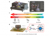
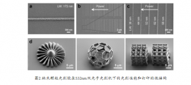
The new energy and materials chemistry team of the Institute of Nuclear Research achieved important results in the field of advanced photoresist
Tsinghua News Network, October 19th Two-photon lithography technology is a micro-nano processing technology with super-resolution characteristics. This photolithography technology uses a high numerical aperture objective lens to focus the excitation beam to form a sub-micron scale focusing point in space, and ultimately achieves fine structure manufacturing through the solubility change of the photoresist during the exposure process. Two-photon lithography can use simple and easily available long-wavelength laser light sources (such as 780nm, 532nm) to break through the diffraction limit with the two-photon focusing effect, achieving ultra-high resolution imaging near EUV lithography level (Note: EUV extreme ultraviolet lithography It is the most advanced photolithography technology in the semiconductor field, but the manufacturing of light sources is extremely difficult and expensive). However, two-photon lithography is a direct engraving technology, and the printing rate is extremely slow, usually only on the micrometer/second to millimeter/second level. When manufacturing larger-volume microstructures, it takes an extremely long writing time, which has become a limitation of two-photon lithography. The bottleneck of large-scale application of photolithography technology (Figure 1c) has not been broken through for more than 30 years.
Recently, the New Energy and Materials Chemistry Team of the Institute of Nuclear and New Energy Technology of Tsinghua University proposed for the first time the mechanism of highly efficient photoinduced polarity changes to regulate the solubility of photoresist, and based on this, successfully developed an ultra-high photosensitivity based on metal oxide nanoparticles. Two-photon photoresist. After testing, the two-photon printing speed using this photoresist reached 7.77m/s. This is the first time in the world that the photolithography speed has been increased to the meter/second level, which is 3-5 orders of magnitude faster than traditional polymer-based photoresists. In addition, the use of this photoresist also achieves extremely high printing resolution, and the line width of the exposed lines can be as small as 38nm, which is better than the line width limit of deep ultraviolet (DUV) immersion lithography technology.


Higher overlay accuracy by design helps boost reliability and higher yields which leads to higher volumes, but I think what Tphuang is saying that "good enough" overlay accuracy plus good scanning speed can also achieve high throughput volume as well, and easier to scale to meet demands today.
I’ll follow up that I think the angle people are missing here is that sometimes, even oftentimes, an improvement in the design point of a performance parameter is an *easier* path to drive production scale than simply trying to figure out how to improve your production engineering to narrower and narrower tolerances. Good engineering solutions are about optimizing for harder and harder conditions. Great engineering solutions are about making high performance easier to engineer. There’s playing to your constraints better and then there’s defeating your constraints. You pick the latter when it’s available every time.
Last edited:
probably from Japan..
if i m not wrong, recently Japan restrict Photoresists sales to China..
******************************************************************
in December 2020, Nata Opto-Electronic announced breakthrough in photoresists in 90-nm, 14-nm and even 7-nm technology nodes. but since then we didn't hear any news.
ArF photoresist plays a protective role against corrosion during the lithography of integrated circuits and it needs to be of high quality. The material can be applied in 90-nm, 14-nm and even 7-nm technology nodes. It can be used to make a wide range of semiconductors, including logic chips, artificial intelligence chips, fifth-generation wireless network chips, large-capacity memory chips and cloud computing chips, the firm said.
Nata Opto-Electronic has invested CNY656 million (USD100.2 million) in the research and development of its own photoresist products. It is aiming to produce 25 tons of ArF photoresist by the end of next year from its plant in Ningbo.
How do we know that NATA isn't simply keeping quiet about their progress in the same way SMEE is?
Is it possibly that they've been secretly producing and supplying SMIC's advanced nodes?
Could be, because their photoresist development is part of project 02 but taking aside ASML SMEE has a monopoly in domestic frontend lithography machines so they can give themselves the luxury of being radio silent about their products because they aren't competing with anybody. NATA in the other hand doesn't have that luxury, more and more domestic companies are launching photoresists for I-line, KrF, ArF and ArFi. So they need to speed the launch of their ArF and ArFi photoresist.How do we know that NATA isn't simply keeping quiet about their progress in the same way SMEE is?
Is it possibly that they've been secretly producing and supplying SMIC's advanced nodes?
How do we know that NATA isn't simply keeping quiet about their progress in the same way SMEE is?
Is it possibly that they've been secretly producing and supplying SMIC's advanced nodes?
NATA is public traded company,SMEE is not. NATA cannot lie to investors by law,so when they tell investors that their product are at verification phase rather than mass produce phase,I'd take their words
Looks like they are getting more money from their ALD-CVD precursor business according to their last statements.
1. Electronic special gases: 1) Hydrogen: Semiconductor grade phospane/arsenane is difficult to supply stably. The company is a leader in this field and plans to add 70 tons of phospane and 30 tons of arsane each to 70 tons. 2) Fluorine: The demand is large and the localization rate is high. The company currently has 4kt of nitrogen trifluoride and 6.1kt of sulfur hexafluoride, leading the country in scale; it plans to add another 7.2kt of nitrogen trifluoride and 500t of sulfur hexafluoride. Tungsten etc.
2. MO source: High R&D threshold and oligopoly. The company achieved a technological breakthrough in 2000 and ranked first in global market share in 2019. The current annual production capacity is 64.9 tons and it is planned to add 13.5 tons.
3. Semiconductor precursors: High-K metal precursors have high technical barriers and few domestic mass-produced companies. The company's related products are already on sale, with a current capacity of 62.5 tons/year and plans to build an additional 113 tons.
4. ArF photoresist: The company is leading in the production and research process. Two products have passed customer verification and have a small number of orders. The company plans to achieve an annual production capacity of 25 tons.
The production capacity of core products has been further expanded, and the production and research of new categories have continued to advance.
1. Electronic special gases: 1) Hydrogen: Semiconductor grade phospane/arsenane is difficult to supply stably. The company is a leader in this field and plans to add 70 tons of phospane and 30 tons of arsane each to 70 tons. 2) Fluorine: The demand is large and the localization rate is high. The company currently has 4kt of nitrogen trifluoride and 6.1kt of sulfur hexafluoride, leading the country in scale; it plans to add another 7.2kt of nitrogen trifluoride and 500t of sulfur hexafluoride. Tungsten etc.
2. MO source: High R&D threshold and oligopoly. The company achieved a technological breakthrough in 2000 and ranked first in global market share in 2019. The current annual production capacity is 64.9 tons and it is planned to add 13.5 tons.
3. Semiconductor precursors: High-K metal precursors have high technical barriers and few domestic mass-produced companies. The company's related products are already on sale, with a current capacity of 62.5 tons/year and plans to build an additional 113 tons.
4. ArF photoresist: The company is leading in the production and research process. Two products have passed customer verification and have a small number of orders. The company plans to achieve an annual production capacity of 25 tons.
TSMC announced its third-quarter results on October 19. Third-quarter net revenue was NT$546.73 billion, a year-on-year decrease of 10.8%, and a month-on-month increase of 13.7%; third-quarter net profit was NT$210.80 billion, a year-on-year decrease of 25.0%, and a month-on-month increase of 13.7%. An increase of 16.0%.
TSMC's gross profit margin for the quarter was 54.3%, operating profit margin was 41.7%, and net profit margin was 38.6%. In the third quarter, 3nm shipments accounted for 6% of total wafer revenue; 5nm accounted for 37%; and 7nm accounted for 16%.
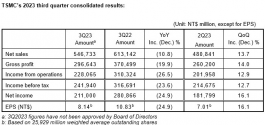
TSMC's gross profit margin for the quarter was 54.3%, operating profit margin was 41.7%, and net profit margin was 38.6%. In the third quarter, 3nm shipments accounted for 6% of total wafer revenue; 5nm accounted for 37%; and 7nm accounted for 16%.

I think it's natural to go there over time. But there are many areas of improvement and improving overlay precision is just one of them. There are many factors that contribute to system up time & yield for a lithography system. I don't pretend that I'm involved in this and would know all those factors. I would presume that overlay accuracy is one of those factors, but I just want to see the system get put into usage and improve rather than being more interested in improving overlay over other areaIf you can chase any productivity or performance improvement in an equipment it improves your your performance and reliability across the board in any application and with that your value proposition to the market.
Think of it this way. If you have a higher overlay accuracy by design that means the production tolerances needed to deliver performance to the lower standard of a previous design point is easier to reach even if you don’t meet your higher design target. Getting greater precision by design *is* how you get to more reliable high volume production.
keep in mind Huawei still uses ARM extensively. In fact, it's more dependent on ARM than almost all other major design houses in China.I would say the writing is on the wall for ARM. Softbank totally mismanaged it.
The botched sale to nVidia, even if it went smoothly was not welcome. No one wanted their competition to control their technology.
Now they are fully public and at the whim of Wall Street. Of course the first order of business was to extort existing customers for increased royalty/licensing payments.
Qualcomm announced the next Snapdragon Wear will be RISC-V (and that means RISC-V Android is nearly complete)
even if they are successful, their planned capacity is just 25t. What can you do with that?How do we know that NATA isn't simply keeping quiet about their progress in the same way SMEE is?
Is it possibly that they've been secretly producing and supplying SMIC's advanced nodes?
Still pretty good numbers in a tough quarter.TSMC announced its third-quarter results on October 19. Third-quarter net revenue was NT$546.73 billion, a year-on-year decrease of 10.8%, and a month-on-month increase of 13.7%; third-quarter net profit was NT$210.80 billion, a year-on-year decrease of 25.0%, and a month-on-month increase of 13.7%. An increase of 16.0%.
TSMC's gross profit margin for the quarter was 54.3%, operating profit margin was 41.7%, and net profit margin was 38.6%. In the third quarter, 3nm shipments accounted for 6% of total wafer revenue; 5nm accounted for 37%; and 7nm accounted for 16%.
View attachment 120317
The only thing long term that would challenge TSMC is SMIC expanding rapidly and soak up all the China OEM demand
- Status
- Not open for further replies.
