Chinese semiconductor industry

Status
Not open for further replies.

european_guy

Junior Member
Registered Member
I don't really see the point of having DUVi machine getting to overlay precision of 2050i. What's the point? You already have enough 2050i. Just have a solid DUVi lithography machine that can cover 40 to 14nm and be used in the DUVi steps of your future 5nm production.

Well, the wafer stage is always the UPrecision's one in all cases. Differently from ASML, SMEE/UPrecision decided to standardize on a single type of stage (cost is not as important, as urgency and also not spreading precious and limited R&D resources, especially at U-Precision).

Moreover ASML will cover 28nm and above also in the future, now it seems "some big fab" will be cut out after the latest round of US bans, but according to ASML CEO this will affect only 15% of ASML's Chinese sales

Moreover Huawei is deeply involved now in SMEE (and for sure they have a say in the roadmap)...and they don't care about mature nodes, they care about 7nm and even lower nodes. For many of their application, from AI to smartphones to data centers to ADAS system for autonomous drive, even 14/16nm maybe not enough.

Moreover the manufacturing capacity at SMEE required for 7/16nm machines is much lower than for 28nm and mature nodes, where Chinese market is able to absorb almost one hundred of machines every year. SMEE cannot cover that for many years to come. Instead the market for advanced litho machines in China is way smaller and SMEE can cover that in pure monopolistic position. This may be easier from the manufacturing capability point of view.
 

tokenanalyst

Brigadier
Registered Member
Well, the wafer stage is always the UPrecision's one in all cases. Differently from ASML, SMEE/UPrecision decided to standardize on a single type of stage (cost is not as important, as urgency and also not spreading precious and limited R&D resources, especially at U-Precision).
SMEE was the one who decided to go with single wafer stage in 2011. U-Precision since the beginning was making dual wafer stages basically since 2014.
 

latenlazy

Brigadier
more importantly, I don't think it really need to be at that level with overlay. I'd rather see a machine that can consistently operate at high work load in volume production of 28nm and 14nm environment. Those are more important factors

I think Paul gets how badly this might play out

if we think that EUV is able to do high volume production in a few years and I think several of us are of that belief

I don't really see the point of having DUVi machine getting to overlay precision of 2050i. What's the point? You already have enough 2050i. Just have a solid DUVi lithography machine that can cover 40 to 14nm and be used in the DUVi steps of your future 5nm production.
The point is that future need for more DUVi isn’t going anywhere just because you have EUV because legacy nodes still benefit from greater overlay accuracy and advanced nodes still use DUVi for lots of patterning steps even if they use EUV to pattern the finest features due to favorable speed and operation cost advantages. This probably will remain true for a while.
 

tokenanalyst

Brigadier
Registered Member

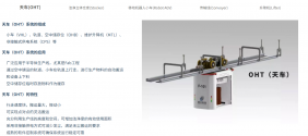
Breakthrough in domestic semiconductor automatic material handling system, "Chengchuan Technology" completed A+ round of tens of millions of yuan in financing​

Chengchuan Technology, a leading domestic semiconductor automatic material handling system (AMHS) overall solution provider, completed tens of millions of yuan in Series A financing. Zhongke Chuang Xingxing, Zhongxin Capital, and Zhongbo invested together, and Shanyun Capital served as the exclusive financial advisor for this round.
Chengchuan Technology was established in 2020 and focuses on providing overall AMHS solutions. Its products and services cover the overall planning and design of AMHS for production lines, the design and manufacturing of automatic material handling and storage equipment, as well as on-site installation and debugging, and the development of software control systems to help customers Improve equipment efficiency and product yield, reduce production costs, and improve manufacturing competitiveness.
At present, the company has delivered 3 complete line projects and obtained final acceptance from customers. The number of delivered cranes exceeds 80, and the length of track delivered is 5,000 meters. Among them, the number of single project cranes is 54, and the track length is nearly 3,000 meters. The person in charge of Chengchuan Technology said that for an advanced packaging factory project that is being implemented, the number of cranes to be delivered will reach 200, with a track length of 10 kilometers, and its scale has reached the level of a wafer factory. If the project is finally delivered successfully, it will become a milestone in the domestic semiconductor AMHS field. In addition, Chengchuan Technology has also achieved technological breakthroughs in the fields of traditional packaging and testing, micro-display, and high-end IC carrier boards.
The founding team of Chengchuan was an established team with more than 15 years of experience in building AMHS at a well-known international semiconductor company. The later members were composed of senior R&D engineers from the automation field and experts from the AMHS department and industry experts of the wafer factory. The team structure is complete and the AMHS system Rich experience in R&D and operation and maintenance.
After the completion of this financing, Chengchuan Technology will continue to expand its team, increase the research and development of core technologies and core products, optimize the supply chain, strengthen interaction with the needs of domestic leading customers, and strive to become a leading company in semiconductor AMHS overall solutions and realize AMHS Comprehensive localization of the system.

1697726353189.png

Please, Log in or Register to view URLs content!
 

tokenanalyst

Brigadier
Registered Member

Jiejia Weichuang successfully shipped large-area perovskite thin film vertical mass production equipment​


Recently, the company successfully shipped large-area perovskite thin film vertical mass production equipment, including RPD and PVD equipment for perovskite. Previously, the company's RPD equipment has been put into use in the customer's perovskite R&D line to help Customers have achieved third-party certified conversion efficiencies of over 19% on perovskite modules.
1697727829780.png

The smooth shipment of the company's RPD and PVD equipment this time marks the company's continued breakthroughs and customer recognition in the perovskite field, as well as repeated orders from customers, and another success in the development of new photovoltaic technologies. At present, the company has the entire line supply capacity of perovskite single-junction cells, all-perovskite stacks, TOPCon stacked perovskites, and HJT stacked perovskites. The RPD equipment that the company focuses on is transparent due to its preparation film layer. With high efficiency, high deposition rate and high conversion efficiency, it has achieved innovative expansion of technology application in the field of perovskite and has been highly recognized by the market. In addition, the company's evaporation equipment, coating equipment, and laser equipment are continuously optimized to meet the individual needs of customers. On this basis, the company innovatively launched a five-in-one clustered perovskite laminated vacuum Coating equipment continues to help customers reduce costs and increase efficiency, and effectively promotes customers' R&D and production in the field of perovskite technology.

Please, Log in or Register to view URLs content!
 

tphuang

Lieutenant General
Staff member
Super Moderator
VIP Professional
Registered Member
The point is that future need for more DUVi isn’t going anywhere just because you have EUV because legacy nodes still benefit from greater overlay accuracy and advanced nodes still use DUVi for lots of patterning steps even if they use EUV to pattern the finest features due to favorable speed and operation cost advantages. This probably will remain true for a while.
I think you misunderstood my post

Is having something with 2050i overlay precision that important for future high volume production?

If you have something more comparable to 1980 or 2000i in overlay, scanning speed and other criteria, is that sufficient for all upcoming processes they may have?

I am more interested in seeing them putting something that can work solidly in high volume production rather than whether or not it can be used in the most critical layer of 7nm process.
 

supersnoop

Major
Registered Member
Please, Log in or Register to view URLs content!

Look like Huawei is designing next generation auto MCU using RISC-V

Certainly a lot of benefit going in this direction vs ARM
I would say the writing is on the wall for ARM. Softbank totally mismanaged it.
The botched sale to nVidia, even if it went smoothly was not welcome. No one wanted their competition to control their technology.
Now they are fully public and at the whim of Wall Street. Of course the first order of business was to extort existing customers for increased royalty/licensing payments.

Qualcomm announced the next Snapdragon Wear will be RISC-V (and that means RISC-V Android is nearly complete)
Please, Log in or Register to view URLs content!
 

latenlazy

Brigadier
I think you misunderstood my post

Is having something with 2050i overlay precision that important for future high volume production?

If you have something more comparable to 1980 or 2000i in overlay, scanning speed and other criteria, is that sufficient for all upcoming processes they may have?

I am more interested in seeing them putting something that can work solidly in high volume production rather than whether or not it can be used in the most critical layer of 7nm process.
If you can chase any productivity or performance improvement in an equipment it improves your your performance and reliability across the board in any application and with that your value proposition to the market.

Think of it this way. If you have a higher overlay accuracy by design that means the production tolerances needed to deliver performance to the lower standard of a previous design point is easier to reach even if you don’t meet your higher design target. Getting greater precision by design *is* how you get to more reliable high volume production.
 
Last edited:

Phead128

Captain
Staff member
Moderator - World Affairs
Higher overlay accuracy by design helps boost reliability and higher yields which leads to higher volumes, but I think what Tphuang is saying that "good enough" overlay accuracy plus good scanning speed can also achieve high throughput volume as well, and easier to scale to meet demands today.
 

latenlazy

Brigadier
Higher overlay accuracy by design helps boost reliability and higher yields which leads to higher volumes, but I think what Tphuang is saying that "good enough" overlay accuracy plus scanning speed can also achieve high throughput volume as well, and easier to scale.
Higher overlay accuracy built into the design means higher scanning speed at lower overlay accuracy than your design point. Increased overlay accuracy expands your acceptable tolerances for mechanical handling and thus how fast you can process the wafers. Overlay accuracy isn’t coming at the expense of speed because the improvement isn’t coming from slowing down the mechanics but improving the precision of the stage control with an inherently better design approach (in this case positional sensor precision). These are expansions in general performance margins not design tradeoffs. When you can get general improvement in broader performance margins around a design point that is *always* the easier solution to scale than trying to optimize a tradeoff, because it can relax the stringency of production tolerances on other mechanical and operational domains. No tradeoff improvements do exist in technological development. It’s how you get the “magic” in technological advancement.
 
Status
Not open for further replies.
Top