Chinese semiconductor industry

Status
Not open for further replies.

olalavn

Senior Member
Registered Member
The official website of the PyTorch Foundation announced today that Huawei has joined the PyTorch Foundation, becoming China's first and the world's tenth PyTorch highest-level Premier member. The official blog stated that Huawei has long been a supporter and contributor to the PyTorch ecosystem. By promoting diverse computing power support and improvements, it has helped more backend manufacturers access the PyTorch ecosystem more easily, and is actively committed to PyTorch optimization. , thereby fully releasing Shengteng’s computing power.

The latest version 2.1 released by the PyTorch community has simultaneously supported Ascend NPU, and with the promotion of Huawei, a more complete third-party device access mechanism has been updated. Based on this feature, third-party AI computing devices can connect to the PyTorch framework without modifying the original framework code. Ascend also provides an officially certified reference implementation of Torch NPU, which can guide third-party devices to easily connect. Based on the new version, users can directly enjoy the native PyTorch development experience on Ascend NPU, and obtain models and applications that run efficiently on Ascend computing devices.
 

tokenanalyst

Brigadier
Registered Member

National Microchip Optical Proximity Correction Platform’s rule-based layout correction tool EsseRBOPC​


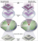
The optical proximity effect refers to the phenomenon that lithography imaging resolution is affected by light diffraction. When the feature size of the mask pattern is smaller than the wavelength of the light, after the light passes through the mask pattern, the light intensity distribution at the corners is mismatched, resulting in edge rounding in the final wafer image compared to the original layout (target pattern) , line end indentation, line width deviation and other distortion issues. Therefore, in order to ensure the reliability of the chip, the OPC (Optical Proximity Correction) tool must be used to correct the mask pattern to compensate for the optical proximity effect and other possible chemical etching effects. The figure below shows the comparison of wafer imaging quality before and after correcting the mask (the red dotted line represents the target pattern).

The "Xintiancheng" platform's rule-based layout correction tool EsseRBOPC (Rule-based Optical Proximity Correction) can provide stable, accurate and high-speed industrial-grade full-chip layout correction solutions for various technology nodes to cope with optical problems in the semiconductor manufacturing process. Problems such as proximity effect, etching effect and yield bottleneck.

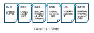
EsseRBOPC workflow
This product is based on distributed computing architecture and heterogeneous task intelligent cluster technology, integrating high-performance unified database, high-performance geometry engine, label engine and regional segmentation engine and other advanced algorithms. It can process ultra-large-scale layout data at high speed and provide complex geometric graphics and Advanced process rules provide high-precision solutions .

1697686608816.png1697686640640.png

Please, Log in or Register to view URLs content!
 

tonyget

Senior Member
Registered Member
It seems that lithography machine is a forbidden topic to talk about,in Chinese semiconductor industry and related academic forum. There seem to be an unspoken official guideline on this,you can find any kind of semiconductor equipment related discussion on various semiconductor forum,Etching/deposition/ion implant etc,but not lithography machine

On "IC world 2023 forum",at the very beginning of this presentation,Dr Zhu Yu from Uprecision said "Six months ago I received invitation to make a speech on this forum. I have been thinking, since lithography machine topic is not allowed to talk about,so what topic should I choose for this presentation?"

Please, Log in or Register to view URLs content!
 

supersnoop

Major
Registered Member
I do agree but there is also what I could call the "early adoption syndrome" where every company just blindly race to be the first to implement out of fear of be left behind.
I still think EUV and its supply chain will get there just it looks like there are some bumps in the beginning of the road.

Not necessarily true, Intel did not have plans to quickly move into EUV and in fact is still only using DUV.

I think the major faulty assumptions made in the article are these:
1. 7nm DUV is not economically viable.
He admits that 7nm is just a rough label. Intel 10nm can be equivalent to 7nm from other foundries based on average feature size and in is now in fact marketed as such (Intel 7)

2. Access to EUV will allow western semiconductor development to hold the lead in the next decade. This could be true, but all it takes is one innovation and a couple setbacks for the competition to catch up or pass you (just ask Intel from above). He even notes the problems with TSMC 3nm.

3. Better performing GPUs will automatically translate to superior ML outcomes. Actually we’ve already seen with crypto and growing data centres that non-technical bottlenecks become an issue. Access to cooling, price of electricity, price of real estate, infrastructure access, etc. The faulty assumption is that people are willing to invest unlimited amounts into AI, when their returns might be better building another self storage warehouse.
 

measuredingabens

Junior Member
Registered Member
Not necessarily true, Intel did not have plans to quickly move into EUV and in fact is still only using DUV.

I think the major faulty assumptions made in the article are these:
1. 7nm DUV is not economically viable.
He admits that 7nm is just a rough label. Intel 10nm can be equivalent to 7nm from other foundries based on average feature size and in is now in fact marketed as such (Intel 7)

2. Access to EUV will allow western semiconductor development to hold the lead in the next decade. This could be true, but all it takes is one innovation and a couple setbacks for the competition to catch up or pass you (just ask Intel from above). He even notes the problems with TSMC 3nm.

3. Better performing GPUs will automatically translate to superior ML outcomes. Actually we’ve already seen with crypto and growing data centres that non-technical bottlenecks become an issue. Access to cooling, price of electricity, price of real estate, infrastructure access, etc. The faulty assumption is that people are willing to invest unlimited amounts into AI, when their returns might be better building another self storage warehouse.
From my understanding in AI the the biggest bottleneck is information transfer, not really raw single card performance. Having great GPUs is all well and good, but that power can't properly be leveraged if they're just sitting idle waiting for data. It's why on the scale of clusters and datacentres the more pressing concern is in networking equipment and other telecom infrastructure and not quite the performance of individual GPUs. It's also why Huawei can be make clusters competitive with the best that Nvidia can put out despite having individually lesser GPUs.
 

Blitzo

Lieutenant General
Staff member
Super Moderator
Registered Member
Rumour
==
According to some sources, the overlay accuracy of the machine has been upgraded to 1.5nm.
Benchmarked asml 2050i to meet the requirements of 5nm process.
The debut is the peak.

Please, Log in or Register to view URLs content!

To be honest this seems a bit too good to be true, albeit probably not outside the realm of technological possibility.
 
Status
Not open for further replies.
Top