Chinese semiconductor industry

Status
Not open for further replies.

siegecrossbow

General
Staff member
Super Moderator
It could be a ban on A800 and H800 or even more restrictions to procure A100 and H100 from intermediaries. Not sure if Alibaba, Tencent and Bytedande have stocked up enough chips and domestic alternatives are widely available yet.
Please, Log in or Register to view URLs content!

Why do these idiots never learn? It is almost a case do sunken cost fallacy with them — we already spent so much money gambling on this approach to work and if we quit now, it would all be for nothing.
 

ZeEa5KPul

Colonel
Registered Member
It could be a ban on A800 and H800 or even more restrictions to procure A100 and H100 from intermediaries. Not sure if Alibaba, Tencent and Bytedande have stocked up enough chips and domestic alternatives are widely available yet.
Please, Log in or Register to view URLs content!
Who called it? Heh, heh, heh:
Please, Log in or Register to view URLs content!
 

Alb

New Member
Registered Member
Please, Log in or Register to view URLs content!

Fellow Choi said, “As a result of analyzing CXMT 21-nano DRAM, it is actually at the level of 18-nano,” and “After U.S. regulations, CXMT does not use numbers (of line width), but is divided into G1 (21-nano), G3 (19-nano), etc. “It appears that the intention is to sell products under 18 nanometers,” he said
 

tphuang

Lieutenant General
Staff member
Super Moderator
VIP Professional
Registered Member
Please, Log in or Register to view URLs content!

Fellow Choi said, “As a result of analyzing CXMT 21-nano DRAM, it is actually at the level of 18-nano,” and “After U.S. regulations, CXMT does not use numbers (of line width), but is divided into G1 (21-nano), G3 (19-nano), etc. “It appears that the intention is to sell products under 18 nanometers,” he said
Very interesting. I wonder what level g3 is at then?

@hvpc any thoughts?
 

tokenanalyst

Brigadier
Registered Member
Can you please elaborate it for the non Chinese speaking people here?

This Tianren Nano volumen nanoimprint machine for 200mm and 300mm substrates, sadly looks in the video are showing the coating system but they didn't showed the patterning system but interesting nevertheless.


GL300 Cluster is a modular, fully automatic nanoimprint production line that integrates a full set of process steps from nanoimprint substrate cleaning, gluing, baking, cooling to nanoimprinting. The standard Tianren Micronano CLIV (Contact Litho in Vacuum) imprinting technology can realize fully automatic high-precision (better than 10nm), high aspect ratio (better than 10:1) nanostructure replication and mass production on a 200/300mm substrate area. . The equipment adopts a modular design. Users can freely configure the number of modules for cleaning, gluing, baking, cooling, Plasma surface treatment, AOI detection, Post Cure and imprinting according to process needs and production rhythm to achieve optimal production efficiency. The equipment supports automatic working mold copying, automatic working mold replacement,automatic preprocessing and imprinting, and automatic demoulding. The entire process is carried out in a closed and clean environment to ensure the quality of the imprinting results.

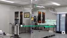
looks like they are planning to introduce more advance systems in the future.

1697136179874.png
 
Status
Not open for further replies.
Top