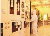
8-inch "Beyond Moore" R&D pilot line to solve the bottleneck of MEMS and silicon photonics technology
Interview background: Shanghai Microtechnology Industrial Research Institute (Chinese abbreviation: Shanghai Industrial Research Institute; English abbreviation: SITRI) was established in 2013 and was initiated by the Shanghai Science and Technology Commission, Jiading District Government and Shanghai Institute of Microsystems and Information Technology, Chinese Academy of Sciences Established as a functional R&D and transformation platform integrating R&D, engineering, industrialization and cultivation, it provides in-depth process technology support and services to innovative enterprises and partners. Under the guidance of the strategic mission of Shanghai Lianhe Investment Co., Ltd. to serve the national strategy and be a pioneer in scientific and technological innovation and development, Shanghai Industrial Research Institute is established based on the "Trinity" innovation architecture model of the Shanghai Institute of Microsystems, Chinese Academy of Sciences, and through the technical strength of the Shanghai Institute of Microsystems. With the support of Shanghai Xinwei Technology Group's investment and operation model, it has established close cooperative relationships with many domestic and foreign industry, academia, and research organizations to achieve high-efficiency industrialization of innovative results and accelerate the establishment of a "Beyond Moore" industrial ecosystem. In order to gain an in-depth understanding of the platform construction and service progress of Shanghai Industrial Research Institute, Memes Consulting recently interviewed the 8-inch R&D pilot line management team.

 What key process developments have been completed in the R&D pilot line so far? What other processes are planned?
In addition to the process accumulation related to integrated circuits, the current R&D pilot line has also developed some special MEMS processes such as SOI, deep silicon etching, glue spraying, wafer bonding, dry film, VOx, AlN, PZT, polyimide, multi-layer optical film growth and etching, etc. These processes have been widely used in pressure sensors, temperature and humidity sensors, infrared thermopiles, uncooled infrared detectors, inertial sensors, microfluidics, genetic testing, virus detection, MEMS speakers and other products.
Because automotive chips are an important direction in the future, we have launched IATF16949 training and enabled the APQP program in project research and development to ensure quality in every step from project evaluation to mass production. Controllable to ensure that the products developed can stably enter mass production.
Piezoelectric MEMS has been very active as a new material MEMS in recent years. In particular, aluminum nitride, as the piezoelectric film material of FBAR, has attracted many technicians to enter this field to start businesses. , which has also caused a large number of investment institutions to invest a large amount of funds in this field.
Silicon photonics is also one of the core technology directions for R&D pilot lines. How is the progress in complete/integrated processes and PDK? Which products have entered the stage of large-scale mass production?
Silicon photonics is a very core technical direction of our R&D pilot line, and it is earlier than MEMS and has a first-mover advantage, so we have invested a lot of equipment in this area, such as ArF lithography machine, Ge/GeSi epitaxy, etc.
that can guarantee 90nm resolution. We released silicon photonics passive PDK 1.0 in 2021, and silicon photonics active PDK 2.0 in 2022. In the fourth quarter of this year, we will release 90nm PDK, and the device library performance indicators will fully reach the international advanced level.


