Chinese semiconductor industry

Status
Not open for further replies.

tokenanalyst

Brigadier
Registered Member

Sai Microelectronics subsidiary established a semiconductor company in Huzhou with a registered capital of 100 million yuan​

Tianyancha shows that Juneng Jingyuan (Huzhou) Semiconductor Materials Co., Ltd. was recently established with a registered capital of 100 million yuan and is 100% controlled by Qingdao Juneng Chuangxin Microelectronics Co., Ltd., a subsidiary of Sai Microelectronics.
The business scope of Ju Energy Crystal Source includes: general projects: research and development of special electronic materials; manufacturing of special electronic materials; sales of special electronic materials; manufacturing of electronic components; wholesale of electronic components; retail of electronic components; technical services, technical development, and technical consulting , technology exchange, technology transfer, technology promotion; import and export of goods, etc.
The business scope of Qingdao Juneng Chuangxin Microelectronics Co., Ltd. is: development and design of electronic products and electronic components; technology development, technology promotion, technology transfer, technology services, technology consulting, and computer technology of radio frequency, analog digital chips, and electronic products. Software, computer system services, application software services, software development, industrial product design; data processing; sales: chips, computer software; import and export of goods and technology, etc.
Recently, Sai Microelectronics stated on the interactive platform that the company's FAB adopts a collinear production model, which can support the process development and wafer manufacturing of various types of smart sensing MEMS wafers; the company is also paying attention to many products including BAW filters. The potential market where industrial demand and domestic substitution demand are superimposed will be combined with market and customer demand to plan existing and future FAB production capacity.

Please, Log in or Register to view URLs content!
 

hvpc

Junior Member
Registered Member
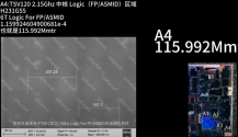
so if you look at his slides. he had High density areas at 115 MMTR and high performance (The big core of CPU) areas at 80 MMTR.
like I said, this incorrect. SMIC N+2 is not at tsmc N7P level in terms of cell size. I would say he is off by about 10%. He may not be aware of the actual feature sizes, and if so I question if he had actually properly determined the transistor density for each die before using it to calculate the number of transistor of each die.
he ended up have N7P and SMIC 7nm at same density. He measured modem and medium cores all at HD density

Looks like he took a thorough look at K9000S. But without knowing how he measured density for different components, I would know idea of how legitimate his numbers are

Also, I don't understand this HP vs HD stuff? Is it common for a decently complex chip like in this case to have a "high performing" density and "high density" density?
Yes. It's up to the fabless guys to decide how to balance between performance and power consumption and optimize to specific application for efficiency and performance. Foundries provide standard logic cell library and the fabless guy decides which logic cell to use in its design. in the case of tsmc 7nm and most likely SMIC, two flavors are offered: 2+2 fin cell for HD & 3+3 fin cell for HP.

HP logic cells is larger than HD logic cells. In tsmc N7P, the HD uses a 2+2 fin configuration while HP uses a 3+3 fin, the latter thus have larger cell height, hence larger unit cell size and lower density. This is why you see a big delta in the process node transistor density number. Typically, we use the HD transistor density number to benchmark different fabs' process node against each other.

I couldn't find the 7nm data, but here's one for tsmc N3 that shows performance of different fin configurations. For N3, there's more flavors, but I think you'll get the jest of the message.1696789330772.png
 
Last edited:

gelgoog

Lieutenant General
Registered Member
It is highly unlikely that the EDA was domestic. But given the increasing amount of silicon design companies in China it is only natural that Chinese EDA will continue to improve. Chinese EDA already enjoys certain niches in chip design as it is with companies like Empyrean having good solutions for analog.
 

sunnymaxi

Major
Registered Member
It is highly unlikely that the EDA was domestic. But given the increasing amount of silicon design companies in China it is only natural that Chinese EDA will continue to improve. Chinese EDA already enjoys certain niches in chip design as it is with companies like Empyrean having good solutions for analog.
There are many Companies..

Huawei's chairman itself announced back in March.


Please, Log in or Register to view URLs content!
MADE BREAKTHROUGHS IN EDA DESIGN TOOLS FOR 14NM CHIPS, SAYS CHAIRMAN XU. Hw have developed PCB, CAD & EDA software for 12/14nm process now. Likely to be validated in SMIC's Finfet process..

***********************************************

Chinese EDA champion Empyrean can now "fully support" 7nm; sees 1Q23 sales growth​


Please, Log in or Register to view URLs content!

**********************************************


Other Chinese EDA progress 鸿芯 w/ 7nm SoC tape-out verification in 2020 By July 2022, it supported Samsung's 5nm process 鸿芯 has full coverage of mature+FinFet product for tape-out verification+mass production Completed >20 local tapeout in past 2 yrs..
 
Last edited:

interestedseal

Junior Member
Registered Member

Skyverse has upgraded and launched new equipment for Lithography metrology.


In 23Q2, the company achieved revenue of 204 million yuan, +170% year-on-year and +26% month-on-month; net profit attributable to the parent company was 15 million yuan,
 
Product iterations and upgrades are smooth, and equipment coverage is expected to be significantly improved. The company attaches great importance to research and development, and the number of R&D personnel has grown steadily: 334 in 23H1, an increase of 12% from 298 in 22H1.

  At the same time, the average salary of R&D personnel increased from 204,900 yuan in 22H1 to 239,400 yuan, which means that the R&D personnel structure has been further optimized. Under the strong R&D background, the iterative upgrades of the company's various equipment are carried out smoothly: 1) Patternless detection: the 1Xnm model has been successfully developed; 2) Pattern detection: models with three-dimensional detection functions have been verified by customers; 3) Three-dimensional topography measurement: Orders are growing steadily; 4) Film thickness measurement: dielectric film thickness actively covers more materials; metal film thickness covers more customer needs; 5) Overlay accuracy: 2Xnm models have been verified by head customers and have won many domestic leading Customer orders; 6) Bright/dark field: 2Xnm bright/dark field detection equipment has been successfully developed; 7) Critical dimensions: 2Xnm critical dimension measurement equipment has been successfully developed.


Please, Log in or Register to view URLs content!
Skyverse isn’t the only company developing overlay metrology tools. Yuwei shipped out its Houyi overlay tool last year. Yuwei also develops mask inspection tools. Mask inspection is rarely talked about but is crucial because one defect on a mask gets copied onto every single wafer produced by it.
Please, Log in or Register to view URLs content!


Please, Log in or Register to view URLs content!
 

tphuang

Lieutenant General
Staff member
Super Moderator
VIP Professional
Registered Member
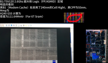
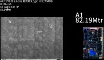
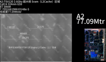
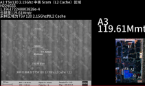
so here is what he posted. Again, very interesting stuff that he claims he found through SEM Analysis. He doesn't have techinsight's credentials, but this is most interesting public available analysis of different part of Kirin 9000S. So, I think this is worth looking over even if we don't accept his measurements

On Baloong Modem he measured about 111.64 Mmtr with 55nm CPP and 240nm cell height
Kirin9000S_SEMAnalysis_BaloongModem.png

This is HP section Taishan big core logic section. measured 82.19 MMTR. is that 328nm cell height?
Kirin9000S_SEMAnalysis_BigCore.png
This is SRAM of Taishan Big core. 324nm cell height. he measured 77.09MMTR
Kirin9000S_SEMAnalysis_BigCoreSRAM.png
 

tokenanalyst

Brigadier
Registered Member

World premiere! Songci’s semiconductor-grade magnetically pulled single crystal furnace received a bulk order from a Korean semiconductor company​


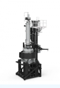
Recently , Songci Electromechanical, a subsidiary of Otway Holding, launched the world's first SC-1600MCZ SEMI semiconductor grade magnetically pulled single crystal furnace and received a batch order for a GQL semiconductor grade single crystal furnace from a subsidiary of DS Techno in South Korea. This is the latest model of Songci Electromechanical. The orders obtained by the semiconductor single crystal furnace from important overseas semiconductor customers are of great significance to the company's business expansion in the semiconductor industry.

Songci Electromechanical has been laying out the technology exploration and research and development of semiconductor equipment since 2020. With its rich semiconductor equipment manufacturing experience and combined with the ever-changing technology accumulation of photovoltaic single crystal furnaces that are currently selling well at home and abroad, Songci Electromechanical has launched the world's first SC-1600MCZ SEMI . The semiconductor-grade magnetic pulling single crystal furnace, with its new structural design, intelligent control system, breakthrough magnetic field control and near-constant pulling speed control, will meet the needs of manufacturing ultra-large silicon wafers of 12-24 inches. Songci Electromechanical's cooperation with GQL, a subsidiary of DS Techno, a Korean semiconductor component company that is a powerful semiconductor company, will further verify the company's R&D results and leading product indicators. The equipment will be fully delivered in March 2024. At the same time, it will help customers build the world's first semiconductor-level unmanned smart crystal pulling factory to reduce costs and increase efficiency, and achieve efficient production.

1696814739184.png
Please, Log in or Register to view URLs content!

 
Status
Not open for further replies.
Top