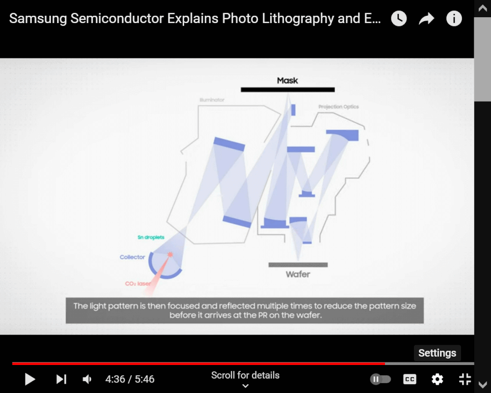
This I never knew. I always assumed the mask was like on top of the wafer, then that gets blasted by the light.
But in ASML black box EUV machine, the mask and wafer are not positioned like that, and what are needed were mirrors and lenses.
Obviously, I got a dumb question, and already assumed my own dumb-ass answer.
If the Chinese really are building a particle accelerator and will harness that EUV light for photo-lithography purposes, then the mask and wafer probably be stacked on top of each other, besides the photoresist and whatever else they have. It will be like a sandwich, and not a complicated reflection process to focus the EUV beam.
Whatever is easier to build, they will build it.
That is why I have my doubts about the Chinese trying to replicate in some form the ASML machine for EUV light. It may be too complicated to reinvent the wheel.
Huawei had to reinvent the wheel, when they made all their modem chips in the Mate 60 Pro. But the modem is kind of like been around.


